



Static Timing Analysis in VLSI: Setup, Hold, Slack, and Timing Closure Explained

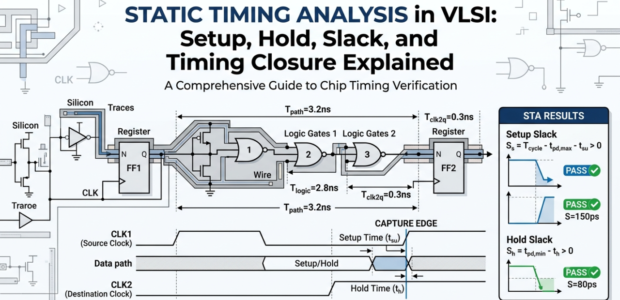
Static Timing Analysis (STA) is one of the most critical steps in modern Very Large Scale Integration (VLSI) digital design. As technology nodes shrink down to deep sub-micron levels, ensuring that a chip functions reliably at its intended operating frequency becomes an intricate challenge. Unlike dynamic timing simulation, which relies on test vectors to verify circuit behavior, STA validates the timing constraints of a design exhaustively across all possible paths without simulating physical operation. For ECE students and entry-level engineers aspiring to build a rewarding career in semiconductor design, mastering STA concepts—specifically setup time, hold time, timing slack, and timing closure—is essential. Understanding these concepts non-dynamically allows timing verification teams to detect potential chip failures early in the design cycle, saving millions of dollars in fabrication re-spins and significantly accelerating time-to-market.
Building a solid foundation in Static Timing Analysis is not only vital for day-to-day design execution but is also a core requirement for cracking technical domain interviews in top semiconductor companies. If you are preparing for entry-level roles in ASIC design, physical design, or timing verification, reviewing the top 50 VLSI interview questions and answers every ECE student should prepare will help you understand how interviewers assess setup and hold concepts. STA acts as the ultimate gatekeeper before tapout, ensuring that data signals arrive neither too late nor too early relative to clock edges. By standardizing timing checks across setup, hold, recovery, and removal conditions, physical design engineers can systematically evaluate performance across various process, voltage, and temperature (PVT) corners. Ultimately, high-grade mastery of timing analysis bridges the gap between theoretical circuit theory and real-world silicon performance, opening prestigious career avenues across global chip design firms.
Summary Comparison of STA Concepts
| Parameter / Metric | Setup Timing Check | Hold Timing Check |
| Core Definition | Data stability required before clock edge | Data stability required after clock edge |
| Check Condition | Max delay path (Worst-Case analysis) | Min delay path (Best-Case analysis) |
| Primary Risk | Data arrives too late | Data arrives too early (race condition) |
| Fix Method | Upsize cells, LVT swapping, pipeline logic | Insert delay buffers, add wire length |
1. Understanding the Fundamentals of Static Timing Analysis (STA)
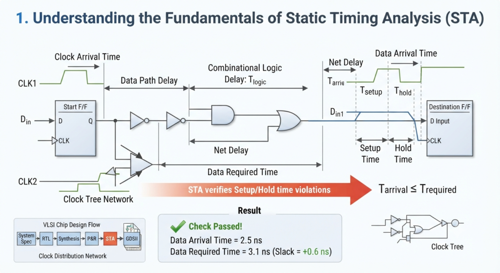
Static Timing Analysis simplifies delay verification by breaking down a complex synchronous design into individual timing paths. Each timing path consists of a startpoint (such as an input port or a register clock pin), combinational logic delays, interconnect propagation delays, and an endpoint (such as an output port or a register data pin). STA calculates the worst-case and best-case delays across these paths and verifies them against pre-defined clock constraints.
By analyzing every path statically, STA provides 100% path coverage without requiring lengthy dynamic test benches. This deterministic approach helps physical design engineers identify critical timing paths, fanout bottlenecks, and high-capacitance nets early in the design cycle, ensuring that signal propagation aligns perfectly with the target operational frequency.
2. Deciphering Setup Time, Hold Time, and Circuit Delays
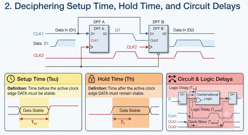
In synchronous digital circuits, flip-flops require stable input data relative to the active clock edge to capture values correctly without entering a metastable state. Setup time ($T_{setup}$) is defined as the minimum duration for which data must remain stable before the active clock edge arrives. Conversely, hold time ($T_{hold}$) is the minimum time data must remain stable after the clock edge. Understanding signal propagation speed and parasite dynamics requires a solid grasp of basic electrical principles; reviewing these basic electrical circuit concepts every VLSI beginner must know will help you better understand resistance, capacitance, and RC propagation delays in timing paths.
Circuit delays in timing paths are broadly categorized into cell propagation delays and interconnect delays. Cell delay depends on input transition time (slew) and output load capacitance, whereas interconnect delay is determined by the resistance and capacitance (RC) of the copper wires connecting logic gates. When data propagates too slowly through heavy combinational logic, setup violations occur. Conversely, if data moves too quickly through fast paths with minimal logic delay, hold violations occur. Physical design engineers carefully balance cell driving strengths, wire routing, and buffer insertion to keep both setup and hold parameters strictly within functional boundaries.
3. Demystifying Setup Slack and Hold Slack Equations
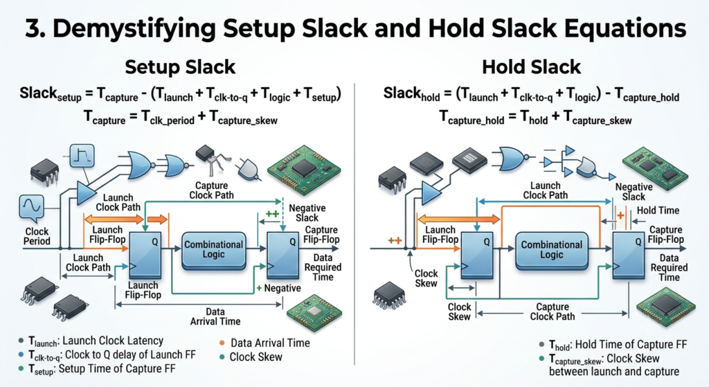
Timing slack is the primary metric used in VLSI design to quantify whether a timing path satisfies or violates required timing constraints. It is mathematically defined as the difference between Required Time (the time by which a signal must arrive) and Arrival Time (the actual time a signal arrives). A positive slack indicates that the path meets timing specifications, a zero slack means the path barely meets timing, and a negative slack signifies a timing violation that must be resolved prior to tape-out.
$$\text{Setup Slack} = \text{Data Required Time} – \text{Data Arrival Time}$$
$$\text{Hold Slack} = \text{Data Arrival Time} – \text{Data Required Time}$$
For setup timing checks, the maximum path delay (worst-case combinational logic and wire delay) is evaluated to ensure data arrives before the next clock edge. For hold timing checks, the minimum path delay (best-case fast path delay) is checked to guarantee data stays stable long enough after the current clock edge. Managing both slack metrics simultaneously across all operational PVT corners is crucial for high-yield silicon execution.
4. Key Strategies for Achieving Timing Closure in Physical Design
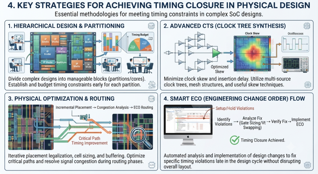
Timing closure is the iterative process of modifying physical design placement, routing, and clock structures until all timing paths demonstrate zero or positive slack across all target operating conditions. Achieving timing closure requires close coordination between synthesis, floorplanning, placement, Clock Tree Synthesis (CTS), and routing stages. Engineers use specialized EDA tools to perform automatic timing-driven optimization throughout the design pipeline.
Common techniques to fix setup violations include gate sizing (up-sizing drivers to reduce logic delay), cell swapping to lower-threshold voltage ($LVT/ULVT$) standard cells, restructuring logic trees, and inserting pipeline registers. To address hold violations—which cannot be fixed by slowing down the clock—designers insert delay buffers along fast paths or adjust clock skew during CTS. Systematic optimization ensures zero setup and hold violations without compromising power consumption or chip area.
5. Industry Tools, Career Scopes, and Practical Best Practices
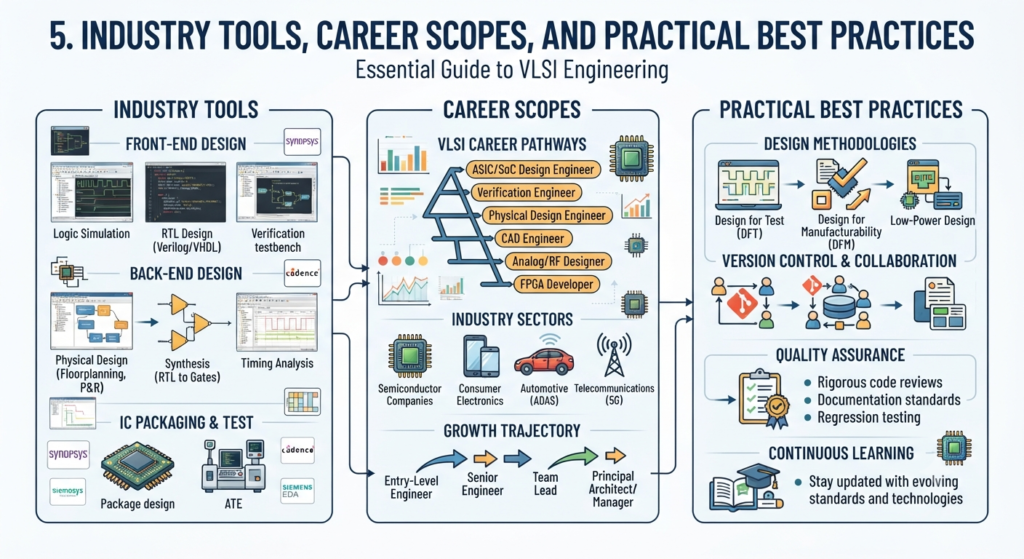
Mastering STA opens up lucrative career pathways in the semiconductor industry, including roles such as STA Engineer, Physical Design Engineer, Synthesis Specialist, and ASIC Sign-off Lead. Leading chip design companies rely on industry-standard EDA tools like Synopsys PrimeTime and Cadence Tempus for sign-off timing analysis. These tools perform multi-scenario timing checks, advanced OCV (On-Chip Variation) modeling, and crosstalk noise analysis to guarantee post-silicon reliability.
For ECE students entering the VLSI domain, building hands-on familiarity with TCL scripting, understanding constraint generation (SDC files), and interpreting STA timing report files are vital career differentiators. Practicing path analysis, understanding derating factors, and keeping up with multi-corner multi-mode (MCMM) closure techniques will position candidate resumes at the top of hiring pipelines in top-tier semiconductor firms.
Conclusion
Static Timing Analysis remains an indispensable cornerstone of modern digital VLSI design, bridging abstract logic verification with realistic hardware timing closure. By thoroughly understanding the nuances of setup time, hold time, timing slacks, and parasitic propagation delays, physical design engineers ensure that complex microchips function reliably under all operating conditions. As semiconductor technology pushes deeper into advanced nodes, expertise in STA sign-off methodologies, OCV modeling, and automated timing closure continues to be one of the most high-demand skill sets in the semiconductor job market. Building strong fundamentals in circuit theory and timing analysis today will pave the way for a successful engineering career in designing the next generation of microprocessors and AI chips.
What is Static Timing Analysis (STA) in VLSI?
Static Timing Analysis is a method of verifying the timing performance of a synchronous digital design by calculating path delays statically without applying test vectors or dynamic logic simulation.
How does setup slack differ from hold slack?
Setup slack measures how much earlier a data signal arrives before the setup window closes, whereas hold slack measures how long a data signal remains stable after the active clock edge.
Why are hold violations considered more critical than setup violations?
Hold violations cannot be fixed by lowering the operating clock frequency post-silicon. If a hold violation exists on chip hardware, it results in catastrophic functional failure, making hold closure imperative before tape-out.
What is On-Chip Variation (OCV) and how does it affect STA?
On-Chip Variation accounts for small process, voltage, and temperature fluctuations across different locations on the same die. STA tools use OCV derating factors to ensure timing margins remain safe under local variation.
Can a circuit have positive setup slack and negative hold slack simultaneously?
Yes, a short combinational path with minimal delay can easily satisfy setup requirements while failing hold requirements if the data changes too quickly after the clock edge.
What is the role of SDC (Synopsys Design Constraints) files in STA?
SDC files define the clock definitions, input/output delay constraints, false paths, multicycle paths, and operating conditions required by EDA tools to execute static timing checks accurately.
Which software tools are widely used for STA sign-off in the semiconductor industry?
The gold-standard commercial tools for STA sign-off are Synopsys PrimeTime and Cadence Tempus Timing Signoff Solution.