



Top 50 VLSI Interview Questions and Answers Every ECE Student Should Prepare

Top 50 VLSI Interview Questions and Answers Every ECE Student Should Prepare
You walk into a chip design interview, the panel opens with “walk me through what happens when you flip a switch on a silicon wafer,” and your mind goes blank. It happens more often than anyone admits.
VLSI hiring in 2026 is not what it was even two years ago. Fabs are racing toward 2nm nodes, AI accelerators are reshaping job descriptions overnight, and recruiters expect sharper, faster answers than a textbook ever taught. This guide breaks down the questions that actually show up in real interview rooms today, organized so you can prepare with intent instead of memorizing random PDFs.
1. Why VLSI Hiring Looks Different in 2026
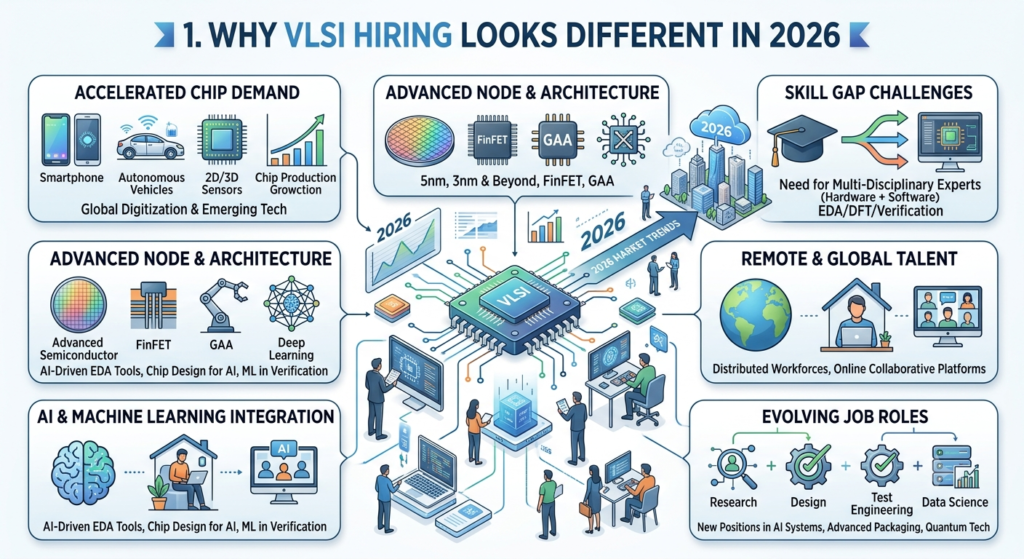
Semiconductor hiring has shifted noticeably this year. Companies aren’t just filling RTL and verification seats anymore — they’re building out teams around chiplet integration, gate-all-around (GAA) transistor architectures, and AI-assisted electronic design automation. That means interview panels increasingly probe whether candidates understand why a design choice matters for power and area, not just whether they can recite a definition. Physical design, DFT, and verification roles are seeing the sharpest demand growth, and panels are testing trade-off thinking — area versus power versus performance versus schedule — far more than they used to. If you walk in only knowing definitions, you’ll struggle the moment the conversation turns to a real design scenario.
2. How a Typical VLSI Interview Is Structured

Most interview loops follow a predictable arc, even if the exact order varies by company. It usually starts with a screening round covering digital fundamentals and a short coding or scripting task, followed by one or two technical rounds that dig into your specialization — RTL, physical design, verification, or analog — and often wraps with a design or debugging problem solved live on a whiteboard or shared screen. Recruiters also increasingly slip in a “tell me about a recent development in the field” question near the end, so staying current on process nodes and packaging trends genuinely pays off. Knowing this structure ahead of time lets you allocate prep time where it counts instead of spreading yourself thin.
3. Core Digital Design and RTL Questions

These fundamentals show up in nearly every interview, regardless of the specific role, because panels use them to confirm your base is solid before going deeper.
Q1. What is VLSI, and why does it matter? VLSI (Very Large Scale Integration) is the process of packing millions to billions of transistors onto a single silicon chip. It’s the reason modern processors, memory, and mobile system-on-chips exist at all — without it, we’d still be wiring together individual discrete components.
Q2. What’s the difference between combinational and sequential logic? Combinational logic output depends only on current inputs, with no memory element involved. Sequential logic depends on current inputs plus stored past states, using flip-flops or latches to hold that history.
Q3. Explain the difference between a latch and a flip-flop. A latch is level-sensitive — it passes data through whenever the enable signal is active. A flip-flop is edge-triggered, capturing data only on a clock edge, which makes it far more predictable in synchronous designs.
Q4. What is setup time and hold time? Setup time is the minimum interval data must be stable before the clock edge; hold time is the minimum interval it must remain stable after. Violating either causes metastability or incorrect data capture.
Q5. What causes a setup violation, and how do you fix it? It happens when data arrives too close to the clock edge, usually from excessive combinational delay. Fixes include re-pipelining the path, upsizing driver cells, or reducing logic levels between flops.
Q6. What is clock skew? Clock skew is the difference in arrival time of the clock signal at different flip-flops. Positive skew can help setup timing but hurt hold timing, and vice versa — it has to be managed carefully across the whole clock tree.
Q7. Define metastability and how designers avoid it. Metastability occurs when a flip-flop’s output settles into neither a clean 0 nor 1 because setup or hold time was violated, often from asynchronous inputs. Designers use double-flop synchronizers to reduce the probability of it propagating.
Q8. What’s the difference between Mealy and Moore state machines? A Moore machine’s output depends only on the current state, giving it more predictable timing. A Mealy machine’s output depends on both state and current input, which can react faster but is trickier to time correctly.
Q9. What is a race condition in digital design? It’s when two or more signal paths compete to change a shared state element around the same clock edge, producing unpredictable results depending on which signal wins. Careful synchronous design avoids relying on such timing coincidences.
Q10. Write the logic for a simple 2:1 multiplexer. out = sel ? in1 : in0; — when the select line is high, the output follows in1; otherwise it follows in0. Interviewers often ask you to extend this to a 4:1 or 8:1 mux to check you understand the scaling pattern.
Q11. What’s the difference between synchronous and asynchronous reset? A synchronous reset only takes effect on a clock edge, which keeps timing clean but needs a stable clock to work. An asynchronous reset takes effect immediately regardless of the clock, which reacts faster but can complicate timing closure.
Q12. What is a finite state machine (FSM), and where is it used? An FSM is a model of sequential logic with a fixed number of states, transitions, and outputs, commonly used to control protocols, arbiters, and datapath sequencing. Interviewers often ask you to design one for a traffic-light-style scenario.
Q13. What’s the difference between blocking and non-blocking assignments in Verilog? Blocking assignments (=) execute sequentially within a procedural block, while non-blocking assignments (<=) schedule updates to happen simultaneously at the end of the time step. Sequential logic should generally use non-blocking to avoid simulation-synthesis mismatches.
Q14. What is a testbench? A testbench is the surrounding simulation environment that generates stimulus, applies it to the design under test, and checks the outputs against expected behavior. It never gets synthesized into hardware — it exists purely for verification.
Q15. Explain the difference between synthesis and simulation. Simulation checks functional correctness by executing the design’s behavior in software over time. Synthesis translates the RTL description into an actual gate-level netlist that can be manufactured, and mismatches between the two are a common source of late-stage bugs.
4. Physical Design, Timing Analysis, and DFT Questions

This is often the round that decides offers, since it tests whether you can turn logic into something that actually works on silicon.
Q16. What are the main stages of the physical design flow? Floorplanning, placement, clock tree synthesis, routing, and signoff, in that general order. Each stage feeds constraints into the next, so a poor floorplan decision early on can create timing or congestion problems that are expensive to fix later.
Q17. What is floorplanning, and why does it matter? It’s the process of deciding the physical placement of major blocks, macros, and I/O pads on the chip. Good floorplanning reduces wire length, congestion, and power delivery issues well before detailed placement even starts.
Q18. What is Clock Tree Synthesis (CTS)? CTS builds the physical clock distribution network so the clock reaches every sequential element with minimal skew and controlled latency. It directly affects both setup and hold timing across the whole chip.
Q19. What is Static Timing Analysis (STA)? STA checks whether every timing path in a design meets setup and hold requirements without running dynamic simulation. It’s exhaustive by construction, which makes it the standard signoff method for timing closure.
Q20. What is a timing path, and what are its components? It’s the route a signal travels from a launch point to a capture point, made up of launch clock delay, data path delay, and capture clock delay. STA compares these against the required timing window to flag violations.
Q21. What causes hold violations, and how are they fixed? Hold violations happen when data arrives at the capture flop too quickly relative to the clock. Common fixes include inserting delay buffers or adjusting clock latency on the affected path.
Q22. What is congestion in physical design, and how do you resolve it? Congestion happens when too many nets compete for limited routing resources in a region, often from dense placement. Resolving it usually involves spreading cells out, adjusting the floorplan, or adding routing blockages strategically.
Q23. What is IR drop, and why is it a concern? IR drop is the voltage loss across the power delivery network as current flows through resistive metal. Excessive IR drop can slow down cells or cause functional failures, so power grid design has to account for worst-case current draw.
Q24. What is Design for Testability (DFT), and why is it needed? DFT adds structures like scan chains and built-in self-test logic so manufactured chips can be tested for defects after fabrication. Without it, detecting a faulty chip on the production line would be nearly impossible at scale.
Q25. What is a scan chain? It’s a technique where flip-flops are reconfigured into a shift-register chain during test mode, letting test patterns be shifted in and captured results shifted out. It dramatically improves fault coverage without needing to access every internal node directly.
Q26. What is ATPG? Automatic Test Pattern Generation is the process of algorithmically creating input patterns that can detect specific manufacturing faults, typically stuck-at or transition faults. It works hand-in-hand with scan chains to achieve high test coverage.
Q27. What is antenna effect in physical design? It’s charge accumulation on long metal wires during fabrication that can damage a connected transistor gate before the chip is fully built. Antenna diodes or jumper wires are common fixes during layout.
Q28. What is crosstalk, and how is it mitigated? Crosstalk is unwanted coupling between adjacent signal wires caused by parasitic capacitance, which can glitch or delay a victim net. Shielding, spacing, and net ordering during routing all help reduce it.
Q29. What is the difference between placement and routing? Placement decides the physical position of standard cells on the die, while routing connects those cells with actual metal wires according to the netlist. Placement quality strongly influences how easy or congested routing turns out to be.
Q30. What is signoff, and what checks does it typically include? Signoff is the final verification stage before tapeout, covering timing (STA), power, IR drop, design rule checks (DRC), and layout-versus-schematic (LVS) checks. Passing every check here is what gives confidence the chip will work as fabricated.
5. Verification, Low Power, and Emerging Technology Questions

Panels increasingly weave in newer topics — advanced packaging, AI-assisted design, and low-power architecture — to see whether your knowledge extends past the classroom basics.
Q31. What is functional verification, and why is it necessary? It’s the process of confirming that a design’s RTL behaves exactly as intended before it goes to fabrication. Since a silicon respin can take months and significant cost, catching functional bugs in simulation is far cheaper than catching them after tapeout.
Q32. What is UVM, and why is it popular? The Universal Verification Methodology is a standardized, reusable framework built on SystemVerilog for building testbenches. It’s popular because it promotes modular, layered environments that scale well across large verification teams.
Q33. What is coverage-driven verification? It’s an approach where functional and code coverage metrics guide how thoroughly a design has been tested, rather than relying purely on directed tests. Verification is considered complete only once coverage goals are met, not just when tests “pass.”
Q34. What’s the difference between formal verification and simulation-based verification? Formal verification mathematically proves properties hold for all possible input combinations, while simulation only checks the specific scenarios you write. Formal is exhaustive within its scope but can struggle to scale on very large designs.
Q35. What is an assertion, and why is it used in verification? An assertion is a statement that checks a specific design behavior holds true during simulation, flagging a failure the moment it’s violated. It catches bugs closer to their root cause instead of surfacing them as a confusing downstream symptom.
Q36. What are the main sources of power dissipation in a CMOS circuit? Dynamic power from switching activity, short-circuit power during transitions, and static leakage power when transistors are idle. Modern low-power designs target all three, since leakage becomes increasingly significant at smaller process nodes.
Q37. What is clock gating? It’s a technique that disables the clock to unused logic blocks when they’re inactive, cutting dynamic power without changing functional behavior. It’s one of the most widely used low-power techniques because it’s relatively simple to implement.
Q38. What is power gating? Power gating shuts off the supply voltage entirely to idle blocks using header or footer switches, eliminating both dynamic and leakage power in that region. It’s more aggressive than clock gating and requires careful state retention planning.
Q39. What is multi-voltage design? It’s an approach where different blocks of a chip operate at different supply voltages depending on their performance needs, reducing overall power. It requires level shifters at voltage domain boundaries to keep signals interpreted correctly.
Q40. What is a GAA (Gate-All-Around) transistor, and why is it relevant now? GAA transistors surround the channel with gate material on all sides, improving electrostatic control compared to FinFETs as nodes shrink below 3nm. Leading foundries are moving to GAA architectures, so panels increasingly expect candidates to know why the shift is happening.
Q41. What is chiplet-based design, and why are companies adopting it? It’s an approach where a chip is split into smaller functional dies manufactured separately and integrated on a single package, rather than building one large monolithic die. It improves yield and lets designers mix process nodes, which is why it’s become central to modern high-performance chip strategy.
Q42. What is advanced packaging, and how does it differ from traditional packaging? Advanced packaging techniques, like 2.5D and 3D integration, stack or place dies much closer together with high-density interconnects, unlike traditional wire-bonded packages. This shortens interconnect distance, cutting both latency and power for die-to-die communication.
Q43. How is AI being used inside the chip design flow itself? Machine learning models are increasingly used for placement optimization, timing prediction, and automated verification pattern generation, cutting design cycle time. It’s shifting some EDA tool interactions from purely rule-based to data-driven optimization.
Q44. What is Design for Manufacturability (DFM)? DFM refers to layout practices that improve yield during fabrication, such as via redundancy, wire spacing rules, and density balancing. It bridges the gap between a functionally correct layout and one that manufactures reliably at high volume.
Q45. What is Low-Power UPF (Unified Power Format)? UPF is a standard format for specifying power intent — voltage domains, power states, and level shifters — separately from the functional RTL. It lets low-power architecture be verified early without having to rewrite the design description itself.
Q46. What is a level shifter, and when is it required? A level shifter converts a signal from one voltage domain to another so it can be interpreted correctly at the receiving end. It’s required at every boundary crossing between blocks operating at different supply voltages.
Q47. What is dynamic voltage and frequency scaling (DVFS)? DVFS adjusts a block’s supply voltage and clock frequency in real time based on workload demand, balancing performance against power. It’s widely used in mobile and edge processors where battery life is a hard constraint.
Q48. What’s the difference between ASIC and FPGA design flows? ASIC design is custom-fabricated silicon optimized for a specific function, requiring a costly and lengthy tapeout process, while FPGAs are reconfigurable hardware that can be reprogrammed after manufacturing. FPGAs are common for prototyping ASIC designs before committing to silicon.
Q49. What is thermal-aware design, and why does it matter more today? It involves placing high-power blocks and managing floorplans to avoid localized hotspots that can throttle performance or reduce reliability. As chips pack more compute into smaller areas, thermal management has become as critical as timing or power closure.
Q50. How should you talk about staying current on industry trends in an interview? Mention specific, recent developments — like the shift toward GAA transistors, chiplet adoption, or AI-assisted EDA tools — rather than a vague claim that you “follow the news.” Naming concrete examples signals genuine engagement with the field rather than a rehearsed answer.
Conclusion
None of these fifty questions matter in isolation — what interviewers are really assessing is whether you can connect a definition to a real trade-off decision under time pressure. Spend your prep time working through why an answer is true, not just what the answer is, and practicing a handful of these out loud with a mock partner. That single habit tends to separate confident, hire-ready candidates from everyone else memorizing the same list the night before.
What are the most common VLSI interview questions for freshers?
Common questions cover Digital Electronics, Verilog, SystemVerilog, CMOS, RTL Design, DFT, Verification, Physical Design, and semiconductor basics.
How should ECE students prepare for a VLSI interview?
ECE students should revise digital electronics, VLSI fundamentals, Verilog, SystemVerilog, CMOS concepts, and practice real-world interview questions.
What VLSI interview questions are asked for freshers?
Freshers are commonly asked about RTL design, logic gates, flip-flops, FSMs, Verilog, CMOS, timing analysis, and basic semiconductor concepts.
Is VLSI a good career for ECE students?
Yes. VLSI offers strong career opportunities for ECE graduates in RTL Design, Verification, Physical Design, DFT, Analog Design, and related semiconductor roles.
What should I study before a VLSI interview?
Focus on Digital Electronics, CMOS, Verilog, SystemVerilog, Computer Architecture, VLSI Design, timing concepts, and basic EDA tools.