
Top 15 VLSI Interview Topics Every Electronics Student Should Master

Entering the semiconductor industry requires a rock-solid foundation in Very Large Scale Integration (VLSI) concepts and practical design methodology. As modern integrated circuits grow exponentially in complexity, semiconductor companies seek candidates who possess deep technical knowledge along with problem-solving skills. Whether you aspire to work in RTL design, functional verification, physical design, or Static Timing Analysis (STA), preparing effectively for technical rounds is critical. Navigating the sheer volume of technical material can feel overwhelming without a structured roadmap to guide your preparation process effectively.
To turn complex chip design concepts into industry-ready skills, structured learning and hands-on practice are essential. Enrolling in an industry-focused program at a reputable VLSI training institute in India can provide the practical exposure and expert mentorship needed to bridge the gap between academic theory and real-world application. A well-designed curriculum helps electronics students tackle difficult interview scenarios with confidence and ease. In this comprehensive guide, we break down the essential topics you need to master to excel in your upcoming VLSI technical interviews.
VLSI Technical Focus Areas: Quick Comparison
| Topic Category | Primary Skills Tested | Key Focus Areas & Concepts | Common Interview Challenge |
| Digital Logic & CMOS | Boolean algebra, CMOS behavior | FSM design, setup/hold times, power dissipation | Solving state reduction & timing hazard problems |
| HDLs (Verilog/SV) | Hardware modeling, Verification | Blocking vs. non-blocking, OOP, constraints | Writing synthesizable RTL for complex logic |
| Static Timing Analysis | Timing validation, Clocking | PVT corners, clock skew, jitter, slack equations | Calculating max frequency from timing paths |
| Physical Design | Implementation, Layout | Floorplanning, CTS, placement, DRC/LVS | Resolving routing congestion & IR drop |
1. Digital Logic Fundamentals and CMOS Basics
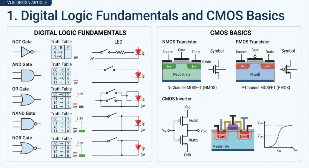
Mastering Boolean algebra, logic gates, flip-flops, and state machines forms the bedrock of all digital design roles. Interviewers routinely evaluate a candidate’s ability to simplify complex logic expressions, analyze setup and hold time requirements, and design robust Finite State Machines (FSMs). Additionally, understanding transistor-level CMOS behavior, noise margins, and power dissipation mechanisms is crucial for resolving low-level implementation challenges during the design process.
In addition to core logic fundamentals, candidates must be ready to solve real-world problem sets during technical rounds. Practicing the top 50 VLSI interview questions and answers every ECE student should prepare ensures you understand how theoretical gate-level concepts are translated into practical interview scenarios. Reviewing these curated questions helps reinforce fundamental problem-solving techniques and improves your confidence when asked to sketch circuit diagrams or analyze timing waveforms live.
2. Hardware Description Languages (Verilog & SystemVerilog)
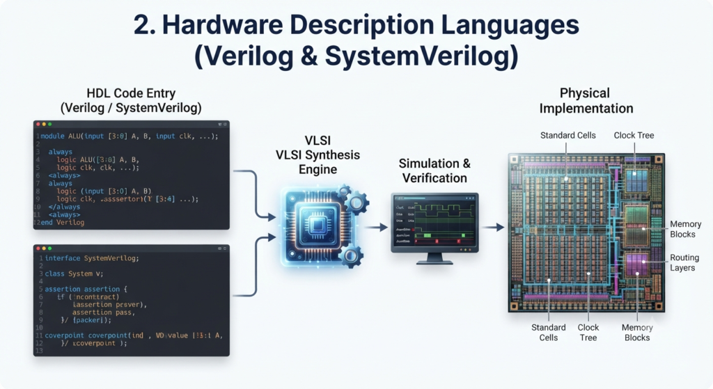
A deep working knowledge of Hardware Description Languages (HDLs) is mandatory for RTL design and verification engineers. You must understand blocking versus non-blocking assignments, synthesis-friendly coding guidelines, parameterization, and hardware modeling techniques. Furthermore, understanding SystemVerilog constructs such as object-oriented programming (OOP), interfaces, constraint random testbenches, and functional coverage is essential for modern verification workflows.
3. Static Timing Analysis (STA) and Timing Closure
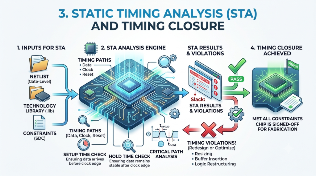
Static Timing Analysis is a core pillar of digital design engineering. Engineers must analyze setup and hold time constraints, clock skew, clock jitter, and propagation delays across different process, voltage, and temperature (PVT) corners. Interviewers frequently present timing paths and ask candidates to calculate maximum operating frequencies or diagnose timing violations such as setup and hold slacks.
4. Physical Design and ASIC Flow Overview
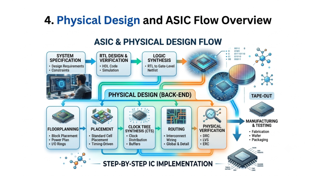
Understanding the complete ASIC design flow—from RTL synthesis and floorplanning to placement, clock tree synthesis (CTS), and routing—is essential. Candidates should understand physical constraints, design rule checks (DRC), layout versus schematic (LVS) verification, and power grid design. Demonstrating clarity on how high-level code translates into physical silicon gives candidates a strong competitive edge.
5. DFT, Testing, and Low-Power Design Techniques
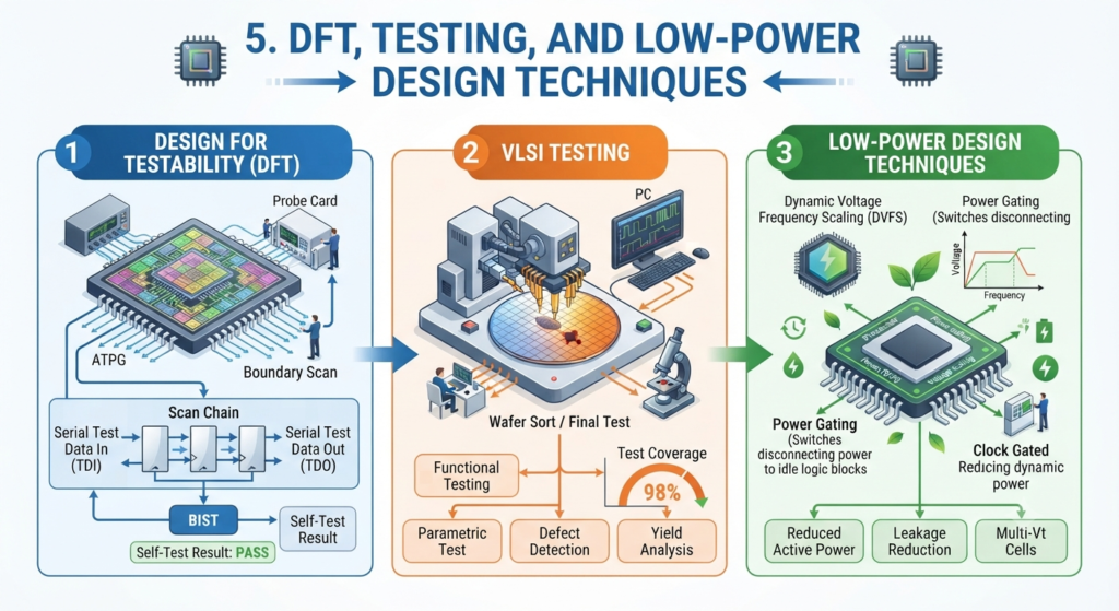
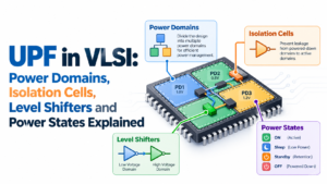
Design for Testability (DFT) techniques like Scan insertion, Built-In Self-Test (BIST), and Automatic Test Pattern Generation (ATPG) ensure manufactured chips are fault-free. Alongside DFT, low-power design methods—including clock gating, power gating, dynamic voltage and frequency scaling (DVFS), and multi-VDD domains—are vital topics frequently explored during advanced technical interviews.
Remaining 10 Essential VLSI Interview Topics
Beyond the core sub-topics detailed above, every electronics student should master these 10 crucial interview areas:
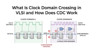
- Clock Domain Crossing (CDC) & Asynchronous Design: Handshake mechanisms, multi-flop synchronizers, FIFO depth calculations, and handling metastability across independent clock domains.
- Finite State Machine (FSM) Optimization: Comparing Mealy vs. Moore architectures, encoding schemes (One-Hot, Binary, Gray code), and avoiding lockup states.
- Setup & Hold Time Violation Fixes: Practical layout and netlist fixes, including buffer insertion, path restructuring, and adjusting launch/capture clock skew.
- Power Dissipation & Optimization: Analyzing static (leakage) vs. dynamic (switching/short-circuit) power dissipation and implementing clock/power gating.
- Verification Methodologies (UVM Fundamentals): Understanding Universal Verification Methodology (UVM) testbench structures, drivers, monitors, scoreboards, and coverage metrics.
- Latch vs. Flip-Flop Inferences: Identifying unintended latch inference in synthesis due to incomplete
if-elseorcasestatements in RTL code. - SRAM & DRAM Architecture: Memory cell structures, read/write stability, sense amplifiers, bank interleaving, and memory built-in self-test (MBIST).
- Cross-Talk & Signal Integrity (SI): Parasitic capacitance extraction, crosstalk noise, glitch propagation, and shielding techniques in high-speed designs.
- Synthesizable vs. Non-Synthesizable Code: Knowing which HDL constructs (e.g., initial blocks, delays
#, system tasks) are simulation-only versus hardware-realizable. - ASIC vs. FPGA Architecture: Differences in LUTs, routing fabrics, configuration cells, hard IP blocks, and trade-offs between NRE cost, unit cost, and flexibility.
1. Why are digital logic fundamentals so critical for VLSI interviews?
Digital logic concepts form the core foundation of hardware design. Interviewers use logic gates, multiplexers, and flip-flop questions to test your fundamental problem-solving abilities before moving to advanced topics.
2. Should an ECE student focus on Verilog or SystemVerilog?
Learning Verilog first is ideal for understanding RTL design fundamentals. However, gaining expertise in SystemVerilog is essential if you wish to pursue roles in functional verification or advanced chip design.
3. What is the difference between Setup Time and Hold Time?
Setup time is the minimum duration data must remain stable before the active clock edge. Hold time is the minimum duration data must remain stable after the active clock edge to ensure correct sampling.
4. What is the role of Static Timing Analysis (STA) in chip design?
STA checks static timing paths across a design without simulating dynamic behavior, verifying that the circuit operates correctly at target frequencies under specified process, voltage, and temperature conditions.
5. Why is clock tree synthesis (CTS) important in Physical Design?
CTS builds a clock distribution network that balances clock delay (insertion delay) to all sequential elements, minimizing clock skew and power consumption across the chip layout.
6. What are the most common low-power design techniques used today?
Clock gating, power gating, multi-threshold CMOS (MTCMOS), and Dynamic Voltage and Frequency Scaling (DVFS) are widely used to reduce both active and leakage power.
7. How does Design for Testability (DFT) help in semiconductor manufacturing?
DFT embeds dedicated test structures (such as scan chains) into the chip architecture, allowing post-silicon manufacturing defects to be identified quickly and reliably.