


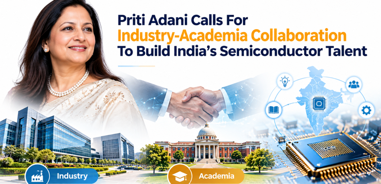
Priti Adani Calls For Industry-Academia Collaboration To Build India’s Semiconductor Talent

The global electronics landscape is experiencing a massive transformation, with semiconductor hardware taking center stage as the bedrock of modern artificial intelligence, telecommunications, and industrial automation. At the Conclave on Hardware, Innovation, Processing and Semiconductor Technologies (CHIPS) 2026, Dr. Priti Adani, President of Adani University, delivered a compelling address highlighting the urgent need for structural synergy between corporate giants and academic institutions. She emphasized that while state-of-the-art fabrication units, assembly facilities, and global investments are essential, the ultimate driver of national self-reliance in Very Large Scale Integration (VLSI) design and hardware engineering remains skilled human capital. Building a resilient domestic chip ecosystem requires moving beyond traditional rote learning toward hands-on talent development tailored specifically to industry demands.
India’s national roadmap under the India Semiconductor Mission (ISM) aims to establish a complete value chain spanning fabless chip design, semiconductor fabrication, and advanced packaging. However, the speed of hardware development continuously threatens to outpace the existing university curricula across the nation. Dr. Adani pointed out that machine intelligence can only advance as far as human intellect can creatively engineer and sustainably guide it. By bridging academia and industrial practice, India can transform its vast pool of engineering graduates into world-class VLSI systems designers, verification engineers, and fabrication specialists. This strategic convergence is critical if the nation is to convert its software dominance into equal hardware leadership on the global stage.
Bridging the Skill Gap in High-Tech VLSI Engineering
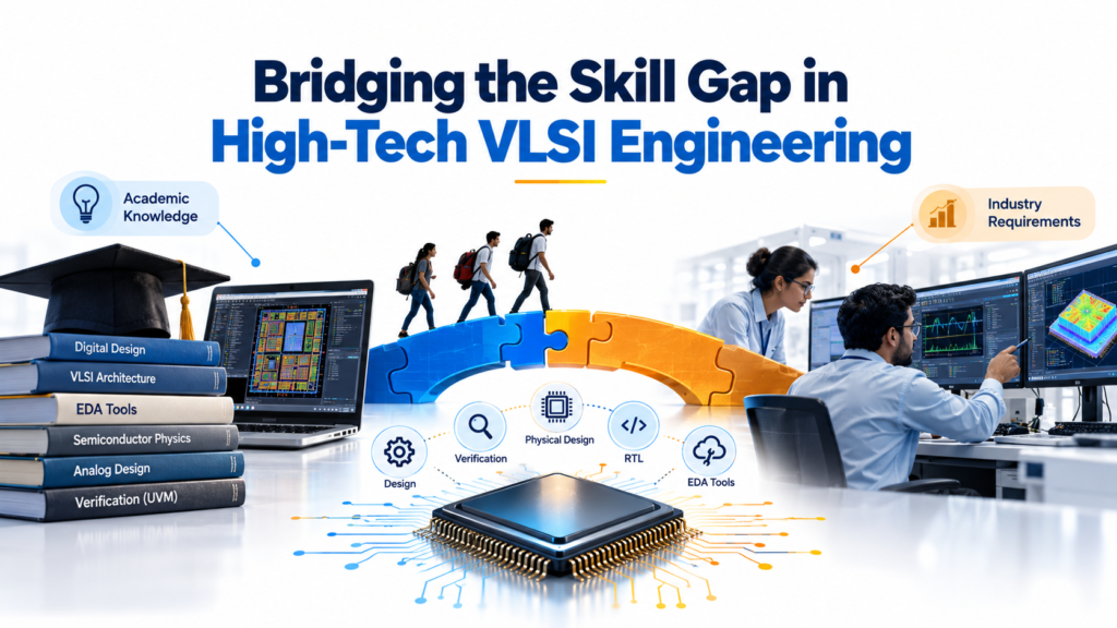
The modern Very Large Scale Integration (VLSI) design cycle demands highly specialized expertise in electronic design automation (EDA), physical design, and static timing analysis. Traditional engineering programs often struggle to mirror the rapid evolution of deep-submicron process nodes used in contemporary semiconductor manufacturing. Without early exposure to modern silicon architectures, engineering graduates face a steep learning curve upon entering the workforce.
To overcome this skill gap, industry-aligned training must be directly integrated into university degree tracks. Establishing specialized semiconductor laboratories, adopting professional EDA toolkits, and involving active industry practitioners in curriculum updates ensure that engineering students work with current fabrication standards. This direct exposure ensures students transition smoothly from theoretical concepts to commercial chip design.
Leveraging the India Semiconductor Mission (ISM) for Workforce Scaling
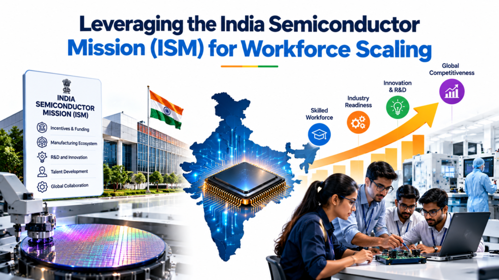
The India Semiconductor Mission (ISM) provides institutional momentum, infrastructure support, and financial incentives to construct an integrated semiconductor supply chain. Crucially, the mission recognizes that long-term sustainability depends on developing a domestic talent pipeline. Major hubs like Dholera and Sanand in Gujarat illustrate how public policy can spur industrial development and create localized demand for skilled engineers.
Expanding academic capability requires aligning national initiatives with regional education hubs. By building dedicated centers for VLSI design, semiconductor packaging, and testing research, academic institutions can supply ready-to-deploy technical talent. Coordinated efforts between state programs and higher education ensure that local infrastructure investments translate directly into sustainable career opportunities for young engineers.
Academic Initiatives and Strategic Curriculum Reform
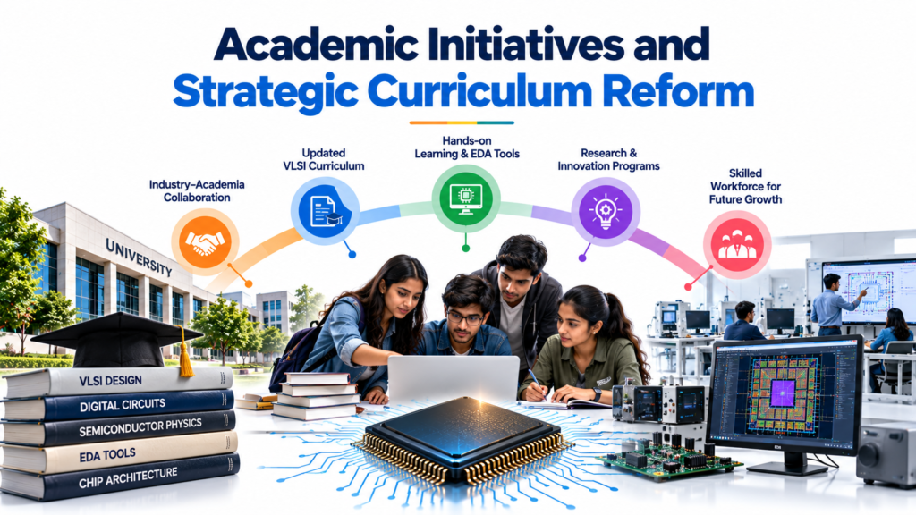
Realizing a world-class semiconductor ecosystem requires fundamental reforms in how technical education is structured. Universities must move beyond general engineering curricula to offer specialized degree paths, executive learning options, and structured faculty development tracks. Teaching the foundations of hardware synthesis, RTL design, cleanroom protocols, and testing prepares students for the realities of modern fab facilities.
Institutions such as Adani University are pioneering industry-focused educational frameworks at specialized campuses. By embedding real-world projects, industrial apprenticeships, and joint research initiatives into the core curriculum, students gain practical exposure to physical design and packaging technologies. This hands-on experience prepares graduates to meet the high quality and performance demands of the global microelectronics sector.
The Expanding Scope: From Chip Design to Advanced Packaging
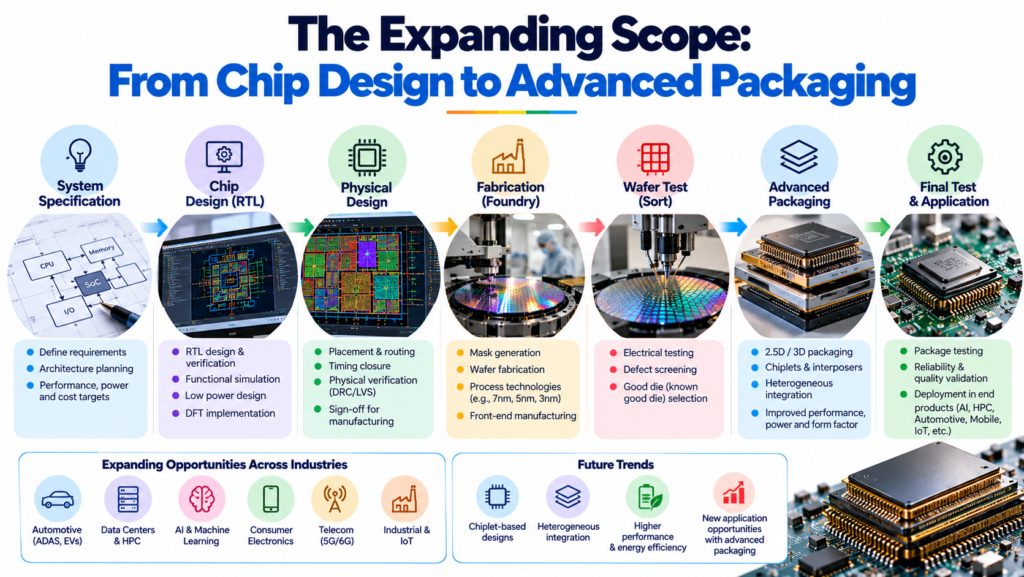
India’s contribution to the microelectronics domain has traditionally focused on front-end fabless chip design. However, modern semiconductor innovation increasingly relies on back-end processes, including Assembly, Testing, Marking, and Packaging (ATMP) and Outsourced Semiconductor Assembly and Test (OSAT) facilities. Advanced multi-chip packaging and heterogenous integration demand strong expertise in thermal management, material science, and signal integrity.
Expanding educational capabilities across the entire semiconductor value chain ensures balanced growth across design and physical implementation. Training engineers in advanced packaging techniques allows domestic facilities to manage complex chiplet architectures locally. Broadening practical training across both front-end and back-end methodologies establishes a complete ecosystem capable of delivering end-to-end silicon solutions.
Global Benchmarks and the Future of Human-Centric AI Hardware
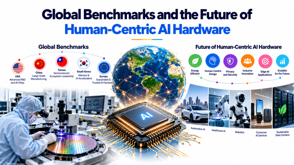
The global demand for advanced hardware is heavily driven by rapid innovations in high-performance computing, generative artificial intelligence, and edge processing. Developing energy-efficient microchips to handle these massive workloads requires specialized talent versed in both hardware architectures and software acceleration. International leaders in microelectronics maintain their edge by continuously funding joint research initiatives between commercial foundries and top-tier universities.
Adopting global industry-academia benchmarks enables domestic institutions to contribute meaningfully to international supply chains. Prioritizing human intelligence alongside machine capability ensures that technological development remains sustainable, secure, and innovative. Cultivating world-class design talent locally positions the nation as a vital partner in the global semiconductor ecosystem.