

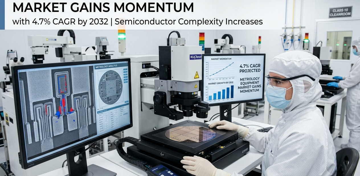
Semiconductor Metrology Equipment Market Gains Momentum with 4.7% CAGR by 2032 | Semiconductor Complexity Increases

If you’ve been following the semiconductor industry, you’ve probably heard about smaller chips, faster processors, and the race for advanced nodes. But here’s what most people miss: none of this is possible without an invisible army of precision measurement tools working behind the scenes. These aren’t just any tools—they’re the metrology and inspection systems that ensure every transistor is exactly where it should be, every layer is precisely the right thickness, and every defect is caught before it becomes a costly problem. The semiconductor metrology equipment market is experiencing unprecedented growth, and this momentum reflects something far more significant than market numbers. It reveals the industry’s acknowledgment that complexity has crossed a threshold where traditional manufacturing approaches simply won’t work. The race to build smaller, faster, and more efficient chips has created an equally intense race to measure and verify them with nanometer precision.
The semiconductor industry currently faces an unprecedented challenge: device complexity is increasing at a pace that’s outstripping the capabilities of yesterday’s inspection methods. Advanced semiconductor manufacturing now involves between 400 to 600 processing steps spread across one to two months of production. A single undetected defect at the early stages can cascade through subsequent manufacturing steps, potentially destroying months of work and millions of dollars in materials. This reality has elevated metrology and inspection equipment from a nice-to-have supportive technology into an absolute necessity for competitive chip production. Market research indicates that leading-edge semiconductor nodes at 7 nanometers and below represent a $5.4 billion segment of the metrology and inspection market, demonstrating how essential these tools have become at the cutting edge of manufacturing.
The Rise of Advanced Node Manufacturing and Its Metrology Demands
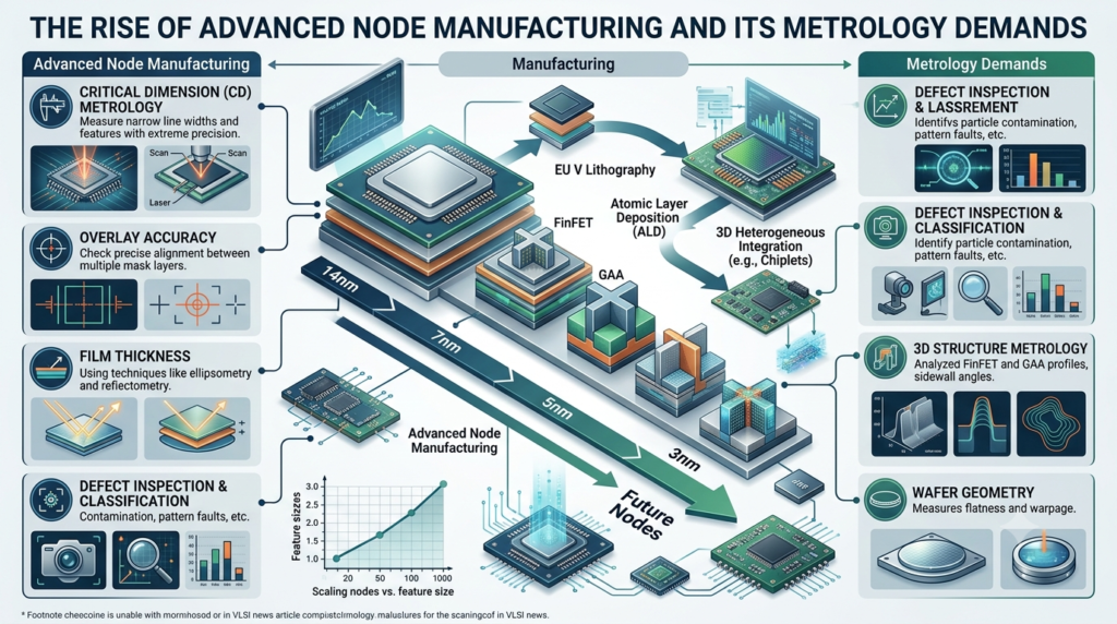
The transition from older process nodes to leading-edge manufacturing represents one of the most significant technological shifts in the industry. As chip manufacturers push toward 2-nanometer and 3-nanometer nodes, the physical dimensions they’re working with approach atomic scales. At these scales, traditional measurement and inspection methods become inadequate. A single rogue atom or misaligned layer can determine whether a chip functions or fails.
The journey toward sub-5 nanometer nodes has exposed fundamental limitations of earlier approaches. Manufacturers now deploy overlay metrology systems to verify that multiple layers align with micron-level precision. They utilize critical dimension metrology to measure line widths that measure just billionths of a meter. Film thickness measurements require tools sensitive enough to detect variations in layers only a few atoms thick. This isn’t theoretical measurement—it’s production-critical functionality that directly impacts chip yield rates. When foundries like TSMC, Intel, and Samsung report yield improvements, those gains trace directly back to better metrology and inspection capabilities catching problems that would have otherwise resulted in scrap wafers.
The market reflects this reality. Current valuations place the semiconductor metrology equipment market at approximately $7 billion in 2024, with projections reaching $12 to $13 billion by 2032. This growth, while appearing gradual in percentage terms, masks an underlying acceleration in technology adoption. Advanced fabs are increasingly implementing automated metrology systems and inline inspection at multiple points during wafer processing. This isn’t just about purchasing more equipment—it’s about fundamentally changing how semiconductor manufacturers approach quality assurance.
Emerging Technologies and Architectural Innovations Driving Equipment Evolution
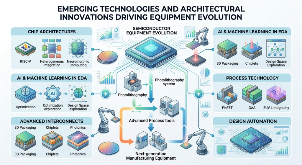
The semiconductor industry’s transition away from FinFET technology toward Gate-All-Around transistor architecture represents a watershed moment for metrology equipment manufacturers. GAA transistors, now entering production at 2-nanometer nodes, require fundamentally different measurement approaches than their predecessors. These nanosheets must be stacked with precision, their dimensions verified at each layer, and the gate material deposited within microscopic gaps that demand measurement tolerances measured in atomic layers.
FinFETs, which dominated the industry since their introduction in 2011, represented a workable compromise between performance and manufacturability. However, as device dimensions shrink below 3 nanometers, FinFETs encounter physical limits that make further scaling impractical. GAA architecture solves this by wrapping the transistor gate completely around the channel in three dimensions, but this creates new measurement challenges. The industry now requires 3D metrology and inspection systems capable of visualizing and measuring structures that exist within complex three-dimensional arrangements.
Simultaneously, memory manufacturers are advancing 3D NAND architecture, stacking layers to unprecedented heights to increase storage density without requiring smaller lateral dimensions. Each additional layer demands precise measurement and verification. This architectural evolution extends beyond logic chips into advanced packaging technologies, where chiplets are bonded together in sophisticated arrangements. These advanced packaging solutions represent some of the fastest-growing segments in the metrology market, requiring tools that can inspect interfaces, verify alignment, and detect defects in three-dimensional packages.
The complexity compounds when manufacturers consider that not every application requires the most advanced nodes. Heterogeneous chip designs now combine cutting-edge logic with mature process nodes, requiring fabs to simultaneously maintain expertise and equipment across multiple technology generations. This diversity in manufacturing creates demand for adaptable metrology platforms that can serve multiple process nodes and applications.
Asia-Pacific’s Dominance and the Global Race for Metrology Capabilities

Asia-Pacific has emerged as the undisputed leader in semiconductor metrology and inspection equipment adoption, commanding over 50% of global market share. This dominance reflects the concentration of advanced semiconductor manufacturing capacity in the region, particularly in Taiwan, South Korea, and increasingly in China. TSMC’s capital expenditure alone—projected at $52 to $56 billion in 2026—flows into the region’s metrology equipment ecosystem, creating a self-reinforcing cycle of innovation and adoption.
Taiwan’s semiconductor ecosystem represents the epicenter of this metrology revolution. TSMC’s transition to GAA at the 2-nanometer node created immediate demand for advanced metrology capabilities that pushed equipment suppliers to accelerate development timelines. Similarly, Samsung’s early adoption of GAA at 3-nanometer nodes positioned South Korea as a crucial testing ground for new measurement technologies. These foundries serve as innovation laboratories where metrology equipment suppliers work closely with manufacturers to solve real-world measurement challenges.
China’s growing semiconductor manufacturing capacity adds another dynamic to regional demand. While Chinese fabs initially operated at mature process nodes, increasing investments in advanced manufacturing capabilities are expanding the addressable market. Equipment suppliers are responding by establishing regional expertise centers and manufacturing hubs to serve Asian customers more effectively.
The regional concentration creates competitive advantages but also highlights geopolitical considerations. Advanced metrology equipment depends on specialized components and expertise that aren’t easily replicated. This concentration of manufacturing capability in Asia-Pacific, combined with global supply chain sensitivities, has made metrology equipment suppliers strategic assets in the broader semiconductor competition between regions.
AI and Automation Transforming Modern Metrology Systems

The integration of artificial intelligence into metrology and inspection systems represents the next frontier in measurement technology. Modern metrology equipment increasingly incorporates machine learning algorithms that can identify defect patterns, predict equipment maintenance needs, and optimize measurement parameters in real-time. These AI-enabled systems don’t just measure dimensions—they interpret data, learn from historical patterns, and make autonomous decisions about which measurements matter most.
Manufacturers report that AI-integrated metrology systems improve defect detection rates while simultaneously reducing false positives that can halt production unnecessarily. Approximately 58% of advanced semiconductor manufacturers have already integrated AI analytics into their inspection workflows, with adoption accelerating as algorithmic sophistication improves. These systems analyze measurement data at scale, identifying correlations between specific defects and upstream process variations that human analysts might miss.
Automation extends beyond measurement into decision-making. Inline metrology systems now automatically flag wafers that exceed acceptable parameter ranges, triggering immediate corrective actions without human intervention. This closed-loop control system enables manufacturers to catch process drifts within minutes rather than hours, preventing entire batches from drifting out of specification before detection.
The convergence of AI and automation creates opportunities for manufacturers to operate with higher productivity while maintaining stricter quality standards. Equipment suppliers are racing to integrate these capabilities, making AI-enhanced metrology a key differentiator in the competitive equipment market.