

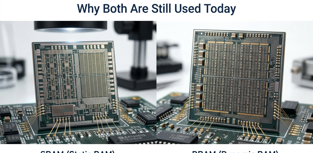
SRAM vs DRAM: Why Both Are Still Used Today

Ever wondered why modern processors pack lightning-fast cache right next to the execution core, yet still rely on separate sticks of system RAM? Despite decades of rapid semiconductor innovation, no single memory technology has been able to offer both ultimate speed and massive, affordable capacity. This fundamental trade-off is why computing architectures still depend heavily on two distinct types of volatile memory: Static RAM (SRAM) and Dynamic RAM (DRAM). Each fulfills a vital role in balancing hardware performance, power efficiency, and manufacturing costs across modern computing systems.
Understanding why SRAM and DRAM continue to coexist requires looking beyond simple speed benchmarks and into their physical design. While SRAM delivers the near-instantaneous access times required for high-speed CPU caches, its large multi-transistor footprint makes it far too expensive for large capacities. Conversely, DRAM provides the dense, cost-effective storage needed for multi-gigabyte system memory, albeit at the cost of higher latency and periodic power refreshing. Together, these two technologies form a complementary memory hierarchy that powers everything from smartphones to AI data centers.
SRAM vs. DRAM: Key Technical & Architectural Differences
| Feature / Characteristic | Static RAM (SRAM) | Dynamic RAM (DRAM) |
| Cell Architecture | Uses a multi-transistor latch/flip-flop circuit (typically 6 Transistors / 6T). | Transistors / 6T).Uses a single transistor and capacitor (1T1C). |
| Data Storage Mechanism | Stored electrically via cross-coupled transistor logic states. | Stored as electrical charge within a microscopic capacitor. |
| Data Refresh Requirement | Stored electrically via cross-coupled transistor logic states. | Stored as electrical charge within a microscopic capacitor. |
| Access Speed & Latency | No refresh required; retains state as long as power is applied | .Requires periodic refresh (hundreds of times per second) due to charge leakage. |
| Storage Density | Ultra-fast (~1 to 10 ns access time). | Moderate / Slower (~10 to 60 ns access time). |
| Cost per Bit | Low density; large physical footprint per bit cell. | High density; extremely small footprint per bit cell. |
| Power Profile | High; expensive due to low density and complex silicon area. | Low; highly cost-effective for large memory volumes. |
| Primary System Use Case | On-chip CPU Cache (L1, L2, L3) and fast execution buffers | .Main System Memory (RAM) modules in PCs, mobile, and servers. |
1. Architectural Differences: Transistor Density vs. Capacitor Refresh
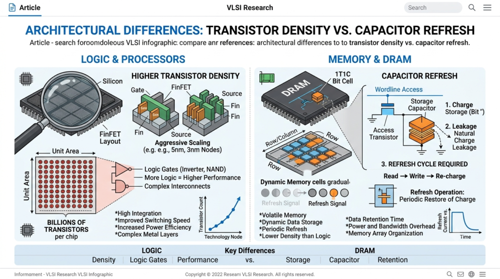
The fundamental difference between SRAM and DRAM lies in their physical bit-cell designs. SRAM utilizes a static latch circuit—typically built using six transistors (6T) per memory bit. This multi-transistor layout holds data stably as long as power is continuously applied, completely eliminating the need to refresh stored charge. Because the state is locked electrically by cross-coupled inverters, SRAM offers exceptional reliability and fast state switching.
DRAM takes a minimalist structural route, using a single transistor and a single tiny capacitor (1T1C) per bit cell. Storing data as an electrical charge inside a miniature capacitor allows DRAM to achieve incredibly high storage density on a single piece of silicon. However, capacitors naturally leak charge over time. To prevent data corruption, DRAM must periodically read and rewrite every cell hundreds of times per second—a requirement known as dynamic refreshing.
2. Performance and Latency: Why SRAM Rules the L1/L2/L3 Cache
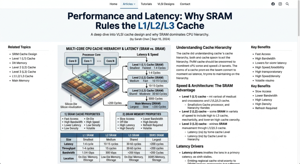
When it comes to raw access speed, SRAM remains completely unrivaled in semiconductor design. Because its 6T bit-cell configuration doesn’t require waiting for a capacitor to charge or discharge, access latency is measured in fractions of a nanosecond. This immediate responsiveness allows SRAM to match the rapid clock cycles of modern CPUs, making it the essential building block for L1, L2, and L3 processor caches.
DRAM operates at significantly higher latency due to its reliance on capacitive charge sensing and complex array matrix routing. Accessing data in DRAM involves opening row address lines, reading delicate charge levels, and buffering data before passing it to the CPU core. This multi-step retrieval process creates a performance bottleneck that would starve high-speed processor execution units if DRAM were used directly as cache memory.
Read more: Embedded C vs C++: Which Programming Language Should Embedded Engineers
3. Cost, Capacity, and Scalability: Why DRAM Dominates Main System Memory
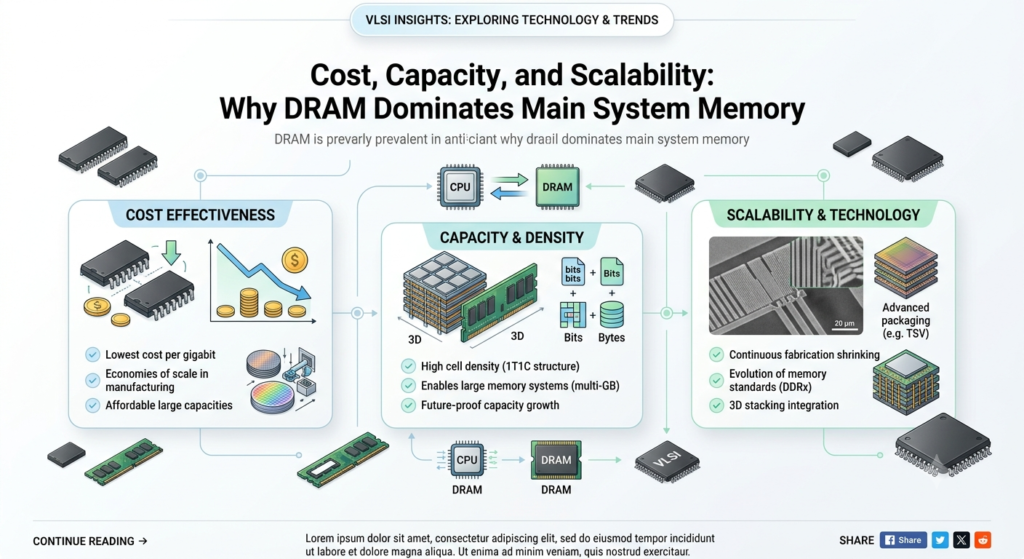
While SRAM excels in execution speed, its physical footprint creates severe scalability limits. A six-transistor cell consumes vast amounts of precious silicon real estate on a die, making high-capacity SRAM exorbitantly expensive to manufacture. Designing hundreds of gigabytes of pure SRAM into a computer would result in massive, unyieldingly costly chips that yield poorly during semiconductor manufacturing.
This is where DRAM’s compact 1T1C architecture demonstrates its massive economic advantage. By shrinking a bit cell down to a single transistor and capacitor, chipmakers can pack billions of storage cells into a tiny area. This extreme density dramatically lowers the manufacturing cost per gigabyte, allowing system builders to supply computers, servers, and smartphones with vast amounts of main system RAM affordably.
4. The 2026 Twist: AI Hardware Is Rewriting the Rules
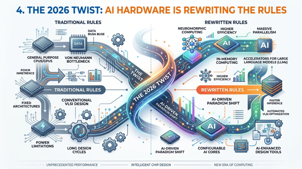
What’s changed recently is how much SRAM some chipmakers are willing to use. AI inference workloads depend heavily on fast access to model weights and intermediate results, and moving that data back and forth from external memory costs both time and power. In response, some newer AI accelerator designs are placing unusually large blocks of SRAM directly on the chip itself, cutting down on data movement instead of relying purely on external high-bandwidth memory stacks.
This shift has been visible across recent industry events, where several AI chip companies have discussed SRAM-centric architectures as an alternative to the GPU-plus-external-memory model that has dominated AI data centers. Some inference-focused chip designers have gone further, treating large pools of on-chip SRAM as a form of main memory rather than just a cache layer, specifically to deal with the huge intermediate data that language models generate while processing a request. Even so, most experts don’t expect SRAM to replace high-bandwidth DRAM technology outright — the two still serve different purposes, with SRAM handling the fastest, most latency-sensitive data and DRAM-based memory carrying the bulk of it.
At the same time, demand for AI memory has become so intense that a broader supply squeeze on DRAM has pushed prices up across laptops, phones, and tablets. Memory manufacturers have been redirecting a growing share of their production capacity toward AI-focused memory, leaving less available for everyday consumer devices, and some industry voices expect that imbalance to persist for several more years rather than resolve quickly.
5. What’s Coming Next: New Memory Tiers
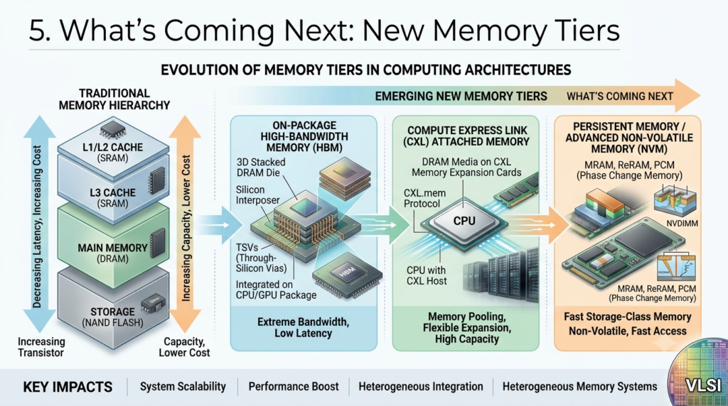
Rather than one technology winning out, the industry seems to be settling into more layers of memory, each tuned for a specific job. Memory makers have been showcasing concepts that sit between ultra-fast stacked memory and high-capacity storage, aiming to combine large capacity with bandwidth closer to what DRAM offers. Packaging techniques that stack memory dies vertically are also improving how efficiently heat and power are managed as these systems get denser.
For everyday devices, this likely means more DRAM tucked closer to processors and smarter cache hierarchies designed to squeeze more performance out of existing SRAM budgets. For large-scale computing, it means memory architecture is becoming as important a design decision as the processor itself, rather than an afterthought bolted on at the end.
Conclusion
SRAM and DRAM aren’t competing for the same job — they’re solving two different problems that both matter. SRAM gives you speed where every nanosecond counts, and DRAM gives you the capacity to hold everything else affordably. That division of labor has held up for decades, and if anything, the demands of AI workloads are making it more relevant, not less. As long as computing keeps needing both instant access and massive storage, SRAM and DRAM will keep working side by side, each doing what the other simply isn’t built for.
1. What is the difference between SRAM and DRAM?
SRAM is faster and does not need constant refreshing, while DRAM is slower but cheaper and denser. SRAM is used for cache memory, while DRAM is widely used as main memory.
2. Why are both SRAM and DRAM still used today?
SRAM offers high speed and low latency, while DRAM provides greater capacity at a lower cost. Their different strengths make both essential in modern computing systems.
3. Which is faster, SRAM or DRAM?
SRAM is faster than DRAM because it uses flip-flop-based memory cells and does not require periodic refreshing, making it ideal for CPU cache and high-speed applications.
4. Why is DRAM cheaper than SRAM?
DRAM uses fewer transistors per memory cell than SRAM, allowing more bits to be stored on a chip. This makes DRAM more cost-effective for large-capacity memory.
5. Where is SRAM used?
SRAM is mainly used in CPU caches, microcontrollers, networking devices, and other applications where fast data access and low latency are important.
6. How do SRAM and DRAM compare in power consumption? SRAM consumes
very little dynamic power when idle because it doesn’t require background refresh cycles, though it experiences static transistor leakage as process nodes shrink. DRAM, on the other hand, constantly draws dynamic power due to the relentless background refresh cycles needed to keep its capacitors charged, even when the system is not actively reading or writing data.
7. How are modern AI workloads changing how chip designers use SRAM? AI
inference and large language models (LLMs) generate massive amounts of intermediate data that demand low-latency processing. To minimize energy-expensive data transfers to external memory, some specialized AI hardware architectures are incorporating significantly larger pools of on-chip SRAM—treating it as ultra-fast local memory rather than just a traditional cache layer.