



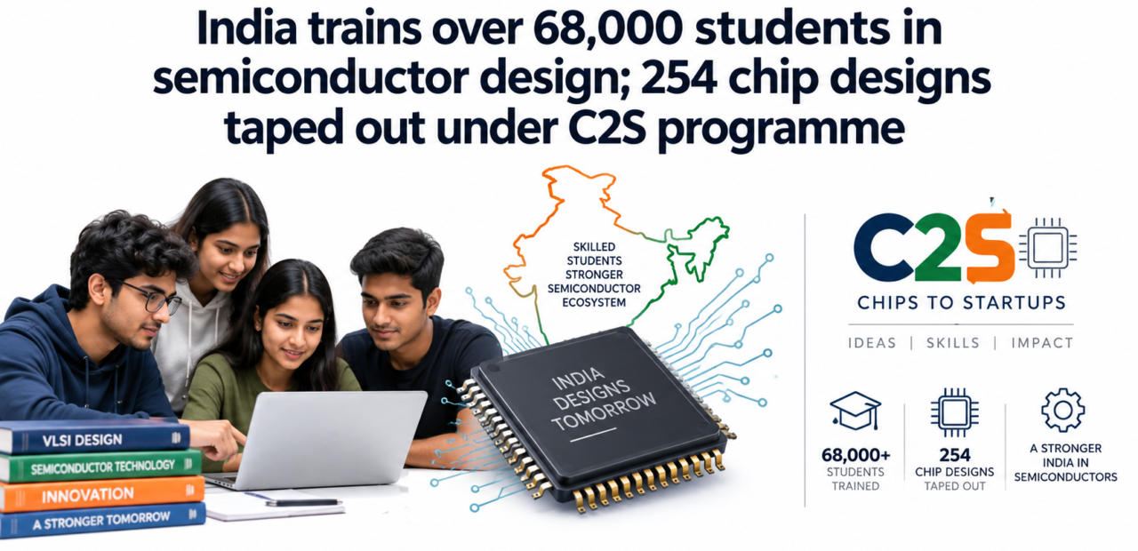
India Trains Over 68,000 in Semiconductor Design; 254 Chip Designs Taped Out Under C2S Programme

A silicon revolution is quietly taking shape in India’s classrooms and labs, and the numbers finally prove it. What was once a country known mainly for writing software for other people’s chips is now designing and taping out chips of its own, at a pace that even a few years ago would have sounded like wishful thinking.
According to the latest update from the Ministry of Electronics and Information Technology, more than 68,000 young engineers have now been trained in semiconductor chip design under the government’s Chips to Start-ups (C2S) Programme. Even more striking, 254 chip designs built by these trainees have been successfully taped out, marking a real, measurable step forward for India’s homegrown chip design ecosystem rather than just another policy announcement.
What the C2S Programme Actually Achieved
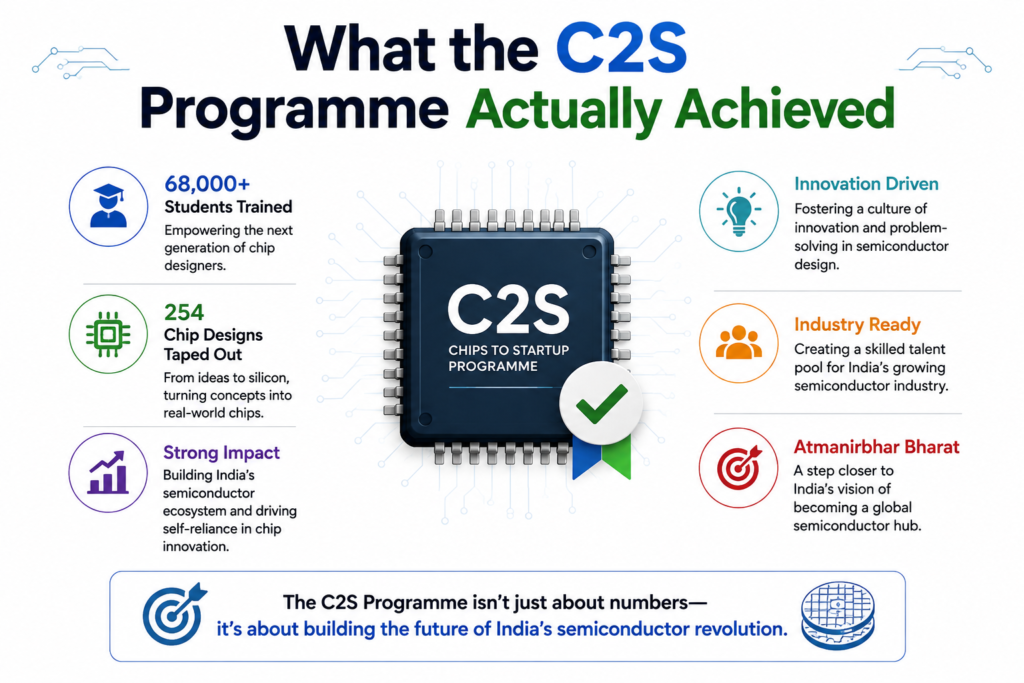
The Chips to Start-ups Programme was launched by MeitY back in December 2021 with a clear mission: build an industry-ready workforce capable of handling the entire semiconductor design lifecycle, from concept to tape-out. Of the 254 total tape-outs recorded so far, 175 designs were completed at the 180 nanometre technology node at the Semi-Conductor Laboratory (SCL) in Mohali, while the remaining 79 were fabricated at overseas semiconductor foundries. That split matters because it shows Indian talent isn’t just getting trained in theory; their work is being validated at both domestic and globally competitive fabrication facilities.
The programme’s broader target is even more ambitious. It aims to generate 85,000 industry-ready professionals across undergraduate, postgraduate, and doctoral levels, including around 200 PhD scholars and thousands of postgraduate specialists focused on VLSI and embedded systems design. Crossing the 68,000 mark shows the initiative is well on track toward that goal, and it signals a maturing pipeline of design talent that India’s chip industry has needed for years.
Why the Tape-Out Numbers Matter More Than the Training Numbers

Anyone familiar with chip design knows that training people is one thing, but getting a design successfully taped out is an entirely different achievement. A tape-out is the final, high-stakes step where a completed chip design is sent to a foundry to be physically manufactured. It requires the design to be functionally verified, electrically sound, and manufacturable at scale, with almost no room for error since a single mistake can mean re-spinning the entire design at significant cost and time loss.
That’s what makes the 254 tape-outs genuinely significant. These aren’t classroom exercises or simulations; they are real silicon, produced through a process that mirrors what professional design teams at global chip companies go through. The fact that 79 of these designs were fabricated overseas at more advanced foundries also suggests Indian design work is increasingly meeting international quality benchmarks, not just domestic ones.
Infrastructure and Tools Powering the Growth

None of this would be possible without serious investment in design infrastructure. The government has extended access to advanced Electronic Design Automation (EDA) tools to 332 academic institutions across the country, sourced from major global players including Synopsys, Cadence, Siemens EDA, Ansys, Keysight, Silvaco, and AMD-Xilinx. These are the same industry-grade tools used by professional chip design teams worldwide, meaning the exposure being provided isn’t a watered-down academic version but the real deal.
This kind of infrastructure access changes the equation entirely. Previously, high-quality EDA tools were prohibitively expensive for most institutions to license independently, creating a major barrier between academic learning and industry-ready skills. By centralising and subsidising this access through the ChipIN Centre, the programme has effectively removed one of the biggest bottlenecks that used to separate classroom design work from real-world semiconductor engineering. Usage of these tools has already crossed 240 lakh hours, an indicator of just how actively the ecosystem is being put to work rather than sitting idle.
What This Means for India’s Semiconductor Ambitions

India currently accounts for roughly 20 percent of the world’s semiconductor design engineers, with more than 1.25 lakh professionals already working in the sector, and the country hosts around 7 percent of the world’s semiconductor Global Capability Centres. Against that backdrop, a steady, verifiable stream of new design talent and successful tape-outs strengthens India’s pitch as a serious hub for chip design, not just chip assembly or testing.
There’s also a startup angle worth watching. Alongside the academic tape-outs, a separate set of 25 chip designs from Indian startups and MSMEs have been taped out through related government schemes, including designs manufactured at advanced nodes such as 12 nanometre facilities. This suggests the pipeline isn’t just producing employable talent for existing companies; it’s also feeding a nascent domestic fabless design industry that could eventually compete on the global stage.
The road ahead still has real challenges. Scaling from 254 tape-outs to a level that meaningfully competes with established design hubs will require sustained funding, deeper industry collaboration, and continued access to cutting-edge fabrication nodes beyond 180 nanometres. But the trajectory is unmistakably positive. What started as a capacity-building exercise is turning into tangible proof that India can design, verify, and manufacture chips end-to-end, and that shift matters far more for the country’s long-term semiconductor ambitions than any single announcement ever could.