


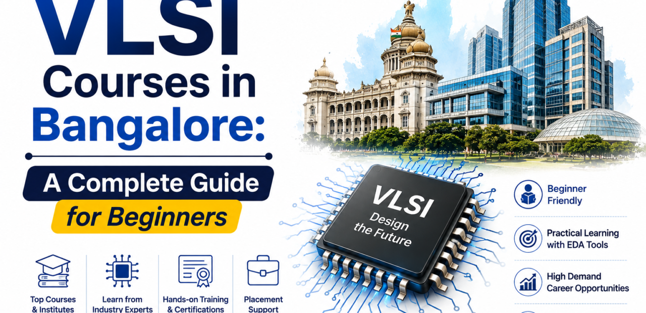
VLSI Courses in Bangalore: A Complete Guide for Beginners

Ever wondered why almost every chip powering your phone, your car, or even your smartwatch has a small piece of Bangalore’s engineering talent behind it? That’s not a coincidence — it’s the result of decades of design work happening quietly in this city, and it’s exactly why so many beginners are now looking at a VLSI course in Bangalore as their entry point into one of the most future-proof careers in technology today.
If you’ve been scrolling through job portals or LinkedIn lately, you’ve probably noticed a pattern: semiconductor and chip design roles keep showing up, and the pay looks nothing like the entry-level jobs your seniors talked about a few years ago. That’s the real pull of a vlsi training institute in Bangalore — it’s not hype, it’s a genuine shift in where the opportunities are heading, and this guide will walk you through everything a beginner actually needs to know before jumping in.
Why Bangalore Is the Right City to Learn VLSI
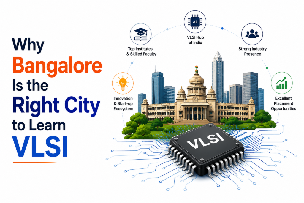
Bangalore isn’t just another city with a few training centers — it’s the operational backbone of India’s chip design ecosystem. Global giants running verification, physical design, and SoC teams out of Bangalore campuses have made it the default hub for anyone serious about a hardware design career. This matters more than most beginners realize, because being physically close to where the actual work happens gives you access to referrals, alumni networks, industry meetups, and internship pipelines that simply don’t exist in smaller tech markets.
There’s also a practical advantage: most training providers in the city design their syllabus around what local companies are actively hiring for, not generic textbook content. So when you enroll in a program here, you’re often learning tools and workflows that mirror what a design or verification team uses on day one of a real job, rather than theory that needs unlearning later.
What a Good VLSI Training Institute in Bangalore Actually Teaches
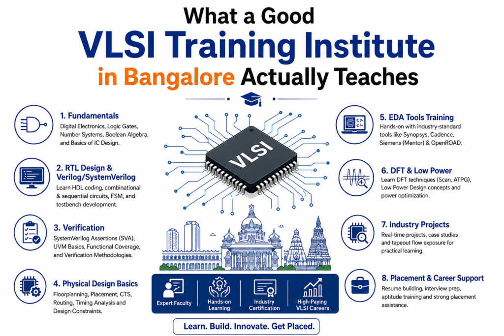
Not all programs are built the same, and this is where a lot of beginners get confused. A solid curriculum usually moves through digital logic fundamentals, Verilog or SystemVerilog coding, RTL design, and then branches into either verification (using methodologies like UVM) or physical design (covering floorplanning, placement, and timing closure). Some institutes also cover DFT (Design for Testability), analog layout, and FPGA-based prototyping, depending on which specialization they focus on.
What separates a genuinely useful vlsi training institute in Bangalore from a mediocre one isn’t the number of tools listed on their brochure — it’s whether you actually get hands-on lab time with industry-standard EDA software, whether your projects resemble real chip development tasks, and whether the trainers have worked inside actual design teams rather than just teaching theory for years. Ask to see sample project work from past batches before you commit; it tells you more about course quality than any marketing page ever will.
Understanding the VLSI Demand in Bangalore Right Now
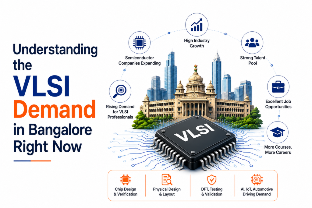
Here’s something worth paying attention to: India’s semiconductor push isn’t a distant policy announcement anymore — it’s actively translating into hiring. New assembly, testing, and packaging facilities are coming online across the country, and while much of that manufacturing is spread across other states, the design and verification work that supports those chips is still heavily concentrated in Bangalore. Companies are increasingly hiring beyond the usual top-tier campuses, which has genuinely widened the door for motivated beginners who can prove their skills through solid projects rather than relying purely on a pedigree.
The vlsi demand in Bangalore today spans multiple layers — verification engineers, physical design specialists, DFT engineers, and analog design roles all show up regularly in hiring listings from major semiconductor firms with design centers in the city. What’s changed recently is the breadth: it’s no longer just a handful of multinational players hiring; homegrown chip design efforts and expanding R&D centers have added more entry points into the field than existed even a couple of years ago.
There’s also a shift in how companies evaluate freshers for these roles. A few years back, a strong academic record alone could open doors. Now, recruiters lean heavily on practical signals — whether you can explain a project you actually built, debug a testbench on the spot, or walk through a timing report without hesitation. This works in favor of anyone who trains seriously, because it means the playing field is less about which college you came from and more about what you can actually demonstrate in an interview room. It’s also why project-based learning has become such a heavily marketed feature across training programs — because it genuinely is what hiring managers are screening for.
How to Choose the Right VLSI Course in Bangalore
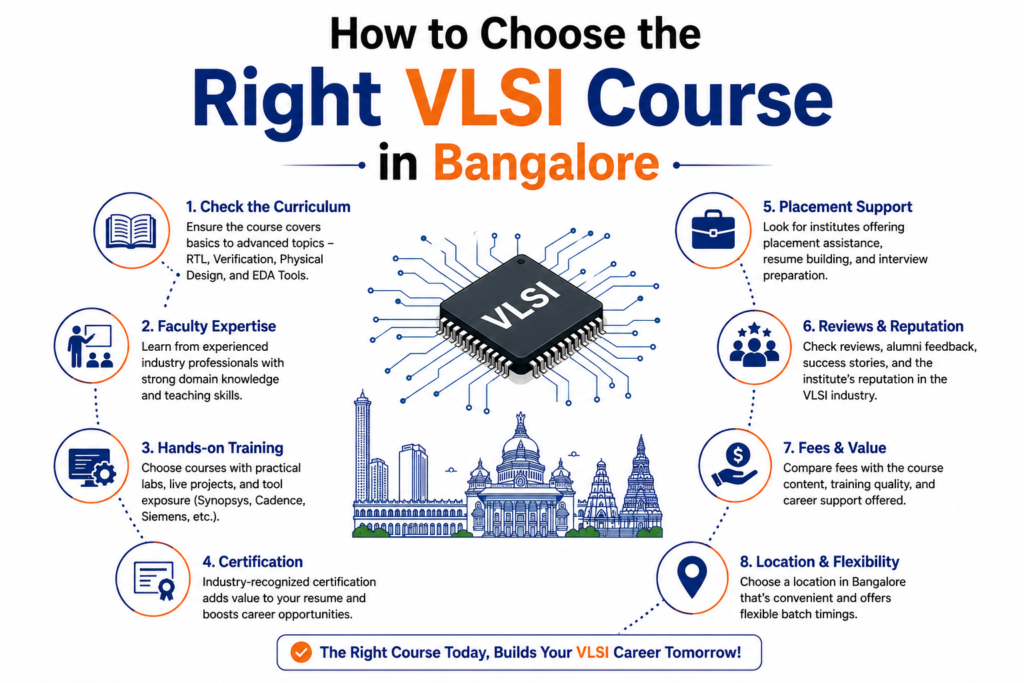
With dozens of institutes competing for attention, picking the right one can feel overwhelming. Start by ignoring flashy placement percentages on their own — ask instead how placements are measured, what roles graduates actually landed, and whether those companies are ones you’d recognize from the industry. A trustworthy vlsi course in Bangalore will be transparent about this instead of hiding behind vague numbers.
Next, look closely at batch size. Smaller batches usually mean more individual attention, especially for debugging sessions where beginners often get stuck. Also check whether the institute offers extended lab access — chip design tools have a learning curve, and cramming everything into scheduled class hours rarely builds real confidence. Finally, talk to a few recent graduates if you can. Their honest feedback about trainer quality, project depth, and post-course support will tell you more in ten minutes than any glossy website will in an hour.
Price matters too, but it shouldn’t be the deciding factor. Course fees vary widely depending on duration and specialization, so instead of chasing the cheapest option, compare what’s actually included — tool access duration, project mentorship, resume support, and mock interview practice all add real value beyond the classroom hours themselves.
Career Path After a VLSI Course: What Comes Next
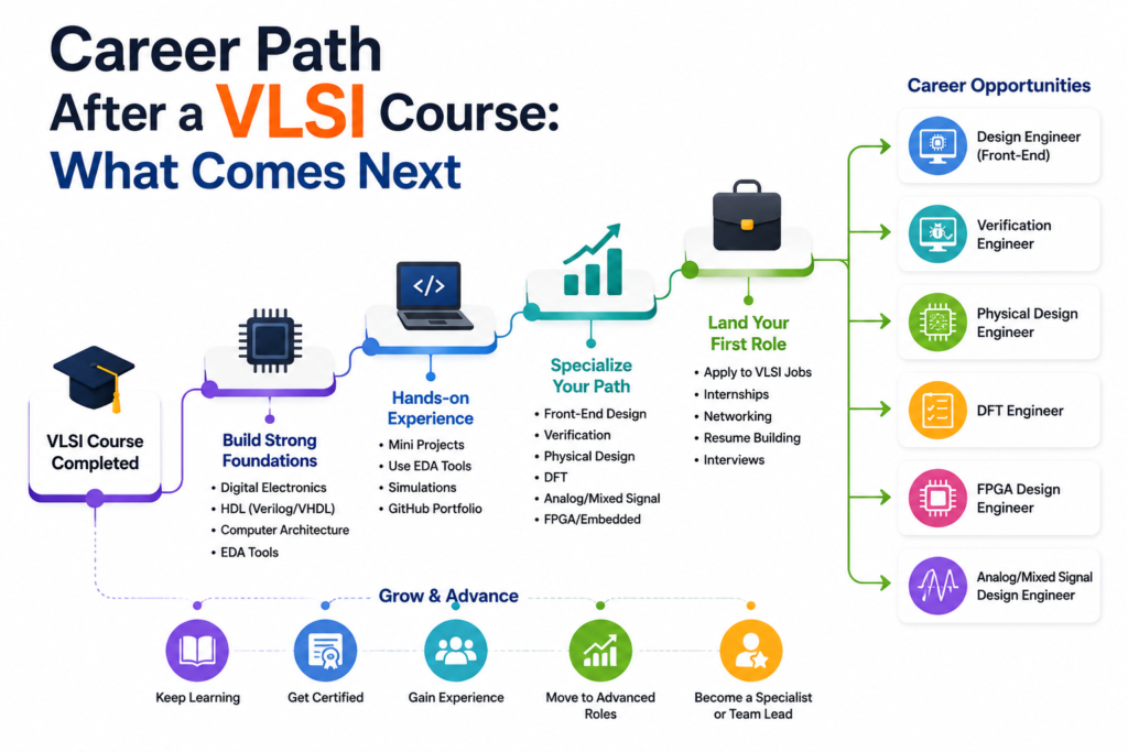
Finishing a course is just the starting line, not the finish. Most beginners enter the field either as verification engineers, working with simulation and testbenches to catch design bugs before a chip goes to fabrication, or as physical design engineers, converting logical circuits into layouts that can actually be manufactured. Both paths offer strong long-term growth, and neither requires you to have prior hands-on chip experience going in — the training itself is designed to bridge that gap.
Beyond the technical roles, there’s also room to grow into DFT, timing analysis, and eventually architecture-level positions as you gain experience. The broader point is that this isn’t a narrow niche career — it’s a layered field with room to specialize based on what genuinely interests you, whether that’s the coding-heavy side of verification or the more visual, layout-driven world of physical design.
Conclusion
Choosing to build a career in chip design isn’t a small decision, but Bangalore genuinely gives beginners one of the best possible starting points in India right now. The city has the companies, the training ecosystem, and the industry momentum all lined up at the same time — something that doesn’t happen in every field. If you go in with realistic expectations, pick a course based on substance rather than marketing, and put in consistent effort on your projects, this is one of those rare moments where the timing and the location genuinely work in your favor.
Take your time researching before you enroll anywhere. Sit in on a demo class if the institute offers one, compare a couple of shortlisted programs side by side, and make sure the specialization you pick actually matches what excites you day to day — because the beginners who stick with this field long enough to build a real career are almost always the ones who chose their path deliberately, not just because it was trending.
1. Which is the best VLSI course in Bangalore?
Choose a VLSI course with hands-on EDA tools, RTL Design, Verification, Physical Design, placement support, and industry-focused projects.
2. Is Bangalore a good place to learn VLSI?
Yes. Bangalore is India’s top semiconductor hub, offering quality VLSI training, internships, and job opportunities with leading chip companies.
3. Can beginners join a VLSI course in Bangalore?
Yes. Most beginner-friendly VLSI courses start with digital electronics and gradually cover RTL Design, Verification, DFT, and Physical Design.
4. Who can enroll in a VLSI course?
ECE, EEE, E&I, Electrical, and related engineering graduates or final-year students can join VLSI courses and start a semiconductor career.
5. How long does a VLSI course in Bangalore take?
Most VLSI training programs last 3–6 months, depending on the specialization, practical labs, and placement assistance.