

Intel and Lens Technology Partner on Advanced Semiconductor Packaging Development

What happens when the world’s oldest chipmaker joins hands with the company that puts glass on your smartphone screen? You get one of the most unexpected — and potentially game-changing — partnerships in the semiconductor world this year. Intel and Lens Technology have just announced a strategic collaboration that could reshape how future AI chips are built, and the story behind it is more interesting than it first appears.
This isn’t just another routine industry tie-up. Intel is betting on glass substrates to solve some of the toughest engineering problems facing modern chip packaging, and it has chosen a company known for precision glass manufacturing to help get there. For anyone tracking the VLSI space, this deal signals where advanced packaging is headed next — and why materials science is quietly becoming as important as transistor design.
The Collaboration at a Glance

Intel Corporation and Lens Technology have entered into a strategic partnership focused on developing next-generation semiconductor packaging built around glass substrates. The two companies announced the collaboration jointly, with Intel bringing decades of experience in chip architecture and packaging, while Lens Technology contributes its background in precision glass processing and laser manufacturing at scale.
The goal is straightforward on paper but ambitious in practice: combine Intel’s packaging know-how with Lens Technology’s material expertise to accelerate the shift toward glass-based packaging solutions. Lip-Bu Tan, Intel’s CEO, described advanced packaging as a critical driver of semiconductor innovation, especially as AI systems continue to demand more performance, scale, and efficiency from the hardware underneath them. Lens Technology’s leadership echoed that sentiment, framing the deal as an opportunity to apply their glass and laser processing capabilities to a completely new industry — semiconductors.
For Lens Technology, this marks a notable pivot. The company has traditionally been associated with consumer electronics, particularly protective glass for phones and tablets. Stepping into semiconductor packaging represents a significant expansion of its business into a far more technically demanding space.
Why Glass Substrates Are Becoming a Big Deal

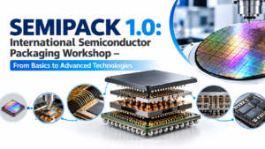
To understand why this partnership matters, it helps to know what problem glass substrates are actually solving. For years, chip packaging has relied on organic substrates to connect and support silicon dies. As chips get more complex and power-hungry — especially the massive AI accelerators used in data centers — these organic materials are starting to hit their limits in terms of flatness, thermal stability, and how tightly interconnects can be packed together.
Glass substrates offer a compelling alternative. They provide better dimensional stability, allow for finer and denser interconnects, and hold up better under the electrical and thermal stress that high-performance chips generate. In simple terms, glass can help pack more computing power into a smaller space without sacrificing reliability, which is exactly what AI, data center, and high-performance computing workloads demand right now.
This is also why the timing of the Intel-Lens deal feels significant. As advanced packaging becomes one of the key ways to keep improving chip performance — especially now that traditional transistor scaling is getting harder and more expensive — companies that master new substrate materials early stand to gain a real competitive edge.
The Role of TGV Technology
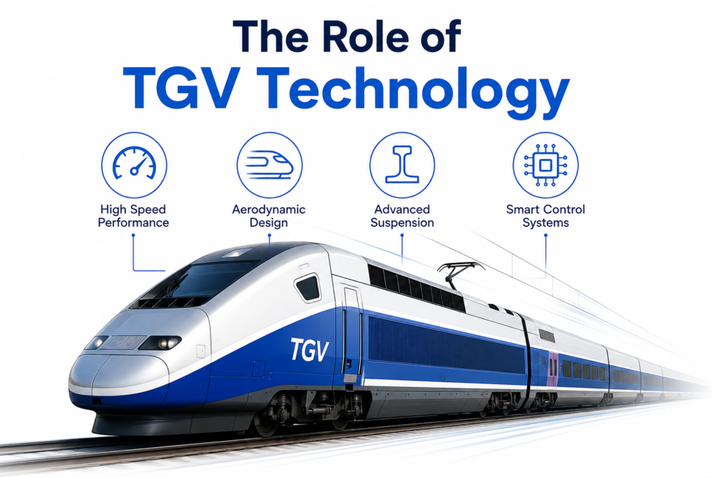
A central piece of this collaboration revolves around Through-Glass Via, or TGV, technology. TGV involves creating extremely precise vertical connections through a glass substrate, allowing signals and power to pass through the material efficiently. This is a technically demanding process that requires exceptional control over drilling, metallization, and structural integrity at a microscopic scale.
Lens Technology’s experience with high-precision laser processing positions it well to tackle this challenge, since TGV manufacturing depends heavily on the kind of fine, controlled material work the company has built its reputation on. Intel, meanwhile, brings its packaging architecture expertise to make sure these glass substrates actually integrate well with real chip designs.
If the collaboration succeeds, TGV-based glass packaging could become a meaningful building block for next-generation processors, particularly those built for AI training and inference, where interconnect density and power efficiency directly affect performance.
What This Means for the Broader Industry

Beyond the technical details, this partnership fits into a larger pattern playing out across the semiconductor industry. Chipmakers are increasingly investing in packaging innovation as a way to extend performance gains, since squeezing more speed purely out of smaller transistors is becoming harder and costlier with each generation.
Intel isn’t alone in this pursuit either. Competitors like Qualcomm and AMD are also investing heavily in advanced packaging techniques, including multi-chiplet designs aimed at improving performance, power efficiency, and scalability. This makes the Intel-Lens Technology partnership as much a competitive move as a technical one — a way for Intel to secure an early foothold in glass substrate manufacturing before rivals do the same.
The potential applications extend beyond just AI chips. Intel and Lens Technology have both pointed to future opportunities in components for AI PCs, thermal and structural solutions for data center servers, and hardware for robotics, industrial equipment, and edge computing. If these areas develop as expected, glass substrate packaging could eventually touch a much wider range of products than just high-end processors.