IBM Reveals Breakthrough Sub-1 Nanometer Chip Technology

What if the next leap in computing power didn’t come from making transistors smaller, but from rethinking how they’re stacked altogether? That’s exactly what just happened. On June 25, 2026, IBM announced it had crossed a threshold the chip industry has been chasing for years: a working sub-1 nanometer chip, built on what the company calls a 0.7 nm, or 7-angstrom, node.
This isn’t a lab curiosity or a distant roadmap promise. IBM says the new chip packs nearly 100 billion transistors onto a piece of silicon the size of a fingernail, roughly double the density of its own 2 nm chip from 2021. For an industry that has spent decades warning that physics would eventually stop Moore’s Law in its tracks, this is a genuinely big moment.
What Exactly Did IBM Announce

At the center of the announcement is a completely new transistor architecture called “nanostack.” Until now, chipmakers have relied on nanosheet designs, where thin films of transistor material are stacked closely on top of one another, wrapped in a gate. IBM’s nanostack takes a different approach: instead of stacking everything in one continuous layer, transistors are staggered across two separate wafers and joined together using a specialized dielectric bond.
Huiming Bu, who leads global R&D for IBM Semiconductors, described it as engineering that operates somewhere between magic and physics. Each transistor sheet is about 5 nanometers thick, roughly 15 atoms, with just 9 nanometers separating the layers. At that scale, the old idea of a “node name” describing an actual physical measurement doesn’t really apply anymore. Node numbers today are more like generational labels for a manufacturing process than literal size specifications, and IBM’s 0.7 nm figure fits that pattern.
Why the Nanostack Design Matters
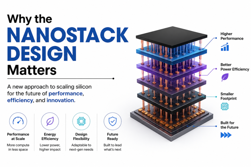
The easiest way to picture the shift is to think of the old nanosheet approach as a simple layer cake, everything piled neatly on top of itself. Nanostack is closer to a checkerboard cake, where sections are staggered and interlocked rather than simply layered. That staggering is what allows IBM to squeeze in far more transistors without hitting the physical wall that comes from just shrinking components further and further.
This matters because for years, the industry playbook was straightforward: shrink the transistor, get more speed and efficiency, repeat. But transistors are now approaching the size of individual atoms, and there’s only so much room left to shrink. Nanostack sidesteps that limit by changing the architecture itself rather than relying purely on miniaturization. It’s a structural innovation as much as a material one, and that’s part of why IBM is framing this as a landmark rather than an incremental update.
Performance Gains and Real-World Impact

Numbers are where this announcement gets genuinely interesting. According to IBM’s published technical results, the new chip could deliver up to 50 percent more performance, or alternatively up to 70 percent greater energy efficiency, compared to its existing 2 nm chips. That’s not a marginal bump; it’s the kind of jump that can reshape what’s possible in data centers, cloud platforms, and edge devices alike.
Jay Gambetta, Director of IBM Research, put it plainly: the goal isn’t just smaller transistors, it’s reinventing how chips are built so they can deliver dramatically more power and efficiency at the same time. That combination, more performance without a matching spike in energy draw, is exactly what large-scale AI training, cloud infrastructure, and next-generation consumer devices need right now. Data centers running massive AI workloads are increasingly constrained by power and cooling, not just raw compute, so a chip that can do more per watt has implications well beyond a spec sheet.
There’s also a broader signal here for anyone watching where computing is headed: gains in generative AI capability have been closely tied to gains in underlying silicon. A more efficient, higher-density node gives model developers and cloud providers more headroom to scale without proportionally scaling their power bills.
What Happens Next and the Road to Production

It’s worth being clear-eyed about timelines. This chip isn’t heading into mass production tomorrow. IBM has stated its goal is to bring the sub-1 nm process into manufacturing within the next five years, and there’s still meaningful engineering work ahead. Bu specifically pointed to challenges like managing thermal noise and integrating the new architecture into existing high-performance computing systems, both of which need to be solved before this becomes a mainstream manufacturing node.
That said, five years is a realistic and fairly aggressive runway for a technology this ambitious, especially given IBM’s track record. The 2 nm chip announced in 2021 has already become an industry reference point, and Gambetta has expressed hope that the sub-1 nm nanostack platform follows a similar path to widespread adoption.
For the semiconductor industry, this announcement is a reminder that the story of chip scaling isn’t over, it’s just changing shape. Instead of squeezing more out of the same basic layout, the next era of progress looks like it will come from rethinking the architecture itself. If IBM’s nanostack approach holds up through the next five years of development, it could set the template that other chipmakers follow as the industry pushes past the nanometer scale entirely and into the realm of atomic-level engineering.
As AI workloads keep growing and power efficiency becomes as important as raw speed, breakthroughs like this one are worth watching closely. This won’t be the last announcement of its kind, but it’s a strong marker of where chip design is headed next.