


How the Semiconductor Industry Is Driving VLSI Career Opportunities in Noida

Ten years ago, if you asked someone in Noida where the city’s engineering jobs were headed, chances are “chip design” wouldn’t have come up. Today it’s a different story. Global fabless giants, established EDA firms, and a wave of new design centers have quietly turned this stretch of Delhi NCR into one of India’s most talked-about semiconductor hubs — and the ripple effect on hiring has been impossible to ignore.
What’s driving this shift isn’t a single factor but a convergence of them: national policy support, proximity to Delhi’s talent and infrastructure, and a genuine global shortage of chip design expertise. For anyone tracking where the next wave of stable, well-paying technology careers will come from, Noida’s semiconductor story deserves a closer look. This piece breaks down exactly what’s happening on the ground and where the real opportunities lie.
Why Noida Has Become a Semiconductor Hotspot

Noida’s rise as a semiconductor destination didn’t happen by accident. The city sits at the intersection of a few advantages that are hard to replicate elsewhere. Its closeness to Delhi gives companies easy access to transport, business infrastructure, and a large pool of engineering talent drawn from across North India. Add to that the push from the India Semiconductor Mission, which has actively encouraged design-services investment, fabless startups, and R&D expansion across the NCR belt, and you get a region that’s growing faster than most people outside the industry realize.
There’s also a strong existing base of IT and electronics companies in and around Noida, which creates a kind of ecosystem effect — talent, vendors, and infrastructure all reinforcing each other. This is why what started as a handful of design offices has turned into a genuine cluster, with more fabrication, assembly, and testing investments reportedly in the pipeline for the region over the next few years.
The Companies Fueling VLSI Job Growth in the Region
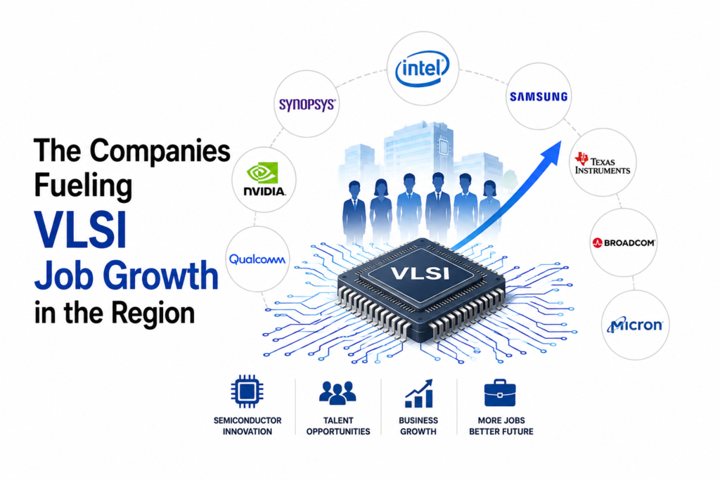
The names driving hiring in Noida’s chip ecosystem read like a who’s who of the global semiconductor world. Multinational players with a strong regional presence are continuously expanding their design and verification teams to keep pace with demand from sectors like automotive electronics, 5G infrastructure, AI hardware, and IoT devices. Alongside them, homegrown technology and engineering services companies have built out dedicated VLSI divisions serving global clients, adding another significant layer of job creation.
What makes this mix valuable for job seekers is variety. Some organizations focus purely on front-end design and RTL work, others specialize in verification and testing, and a growing number are building capability in physical design and DFT (design for testability). This spread means there isn’t just one entry point into the industry — there are several, depending on where your interests and strengths lie. And because so many of these companies operate on global product timelines, the work itself tends to be fast-paced and genuinely cutting-edge rather than routine maintenance.
It also helps that the region isn’t dependent on a single sector for demand. Automotive electronics teams need engineers who understand safety-critical design constraints, telecom-focused groups are hiring around 5G and network infrastructure chips, and a newer wave of AI hardware startups is looking for talent comfortable with high-performance, power-efficient architectures. This diversification means that even during slower hiring cycles in one sector, opportunities in another tend to keep the overall market fairly resilient — something that’s becoming an increasingly attractive quality in today’s job market.
In-Demand VLSI Skills Employers Are Hiring For Right Now
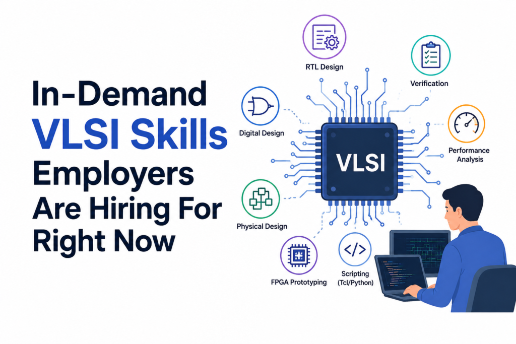
If there’s one thing recruiters in this space agree on, it’s that raw technical depth still wins over generic qualifications. Employers are actively looking for strength in digital design and RTL coding using Verilog and SystemVerilog, along with solid grounding in functional verification methodologies such as UVM. Physical design know-how — covering synthesis, place-and-route, and timing closure — is another area where demand consistently outpaces the available talent pool.
Beyond the core design tracks, low-power design techniques and SoC architecture understanding have become increasingly valuable as chips pack in more functionality while consuming less power. Familiarity with industry-standard EDA tools from major providers is often expected, and scripting ability in Python or similar languages helps candidates stand out in verification and debugging-heavy roles. Interestingly, DFT continues to be one of the more underserved specializations — fewer professionals build deep expertise here, which often translates into a pay premium for those who do.
It’s also worth noting that soft skills carry more weight in this field than outsiders often assume. Chip design is rarely a solo activity — engineers work in close coordination with cross-functional teams spread across time zones, which means clear documentation and the ability to explain technical trade-offs simply are valued almost as much as coding speed. Employers reviewing applications for VLSI roles increasingly look for evidence of applied project work rather than certificates alone, so building even a small portfolio of design or verification projects can meaningfully improve interview outcomes.
Salary Trends and Growth Potential in Noida’s VLSI Sector

Compensation in this field has been trending upward, and Noida is very much part of that story given its concentration of design centers. Entry-level roles typically open the door to steady, above-average starting packages compared to many other engineering fields, while professionals who build three to five years of hands-on design or verification experience often see a sharp jump in earning potential. Those who move into specialized or leadership-track roles — particularly in analog design, AI chip architecture, or advanced verification — tend to command the highest packages in the industry.
What makes the growth trajectory particularly appealing is its consistency. Because chip design skills are transferable across industries — automotive, telecom, consumer electronics, defense — professionals aren’t limited to one type of employer. This flexibility, combined with the sheer scale of global demand for semiconductor talent, is part of why so many technology professionals are actively considering a shift into this space rather than staying in more saturated software roles.
How to Start or Switch Into a VLSI Career in Noida
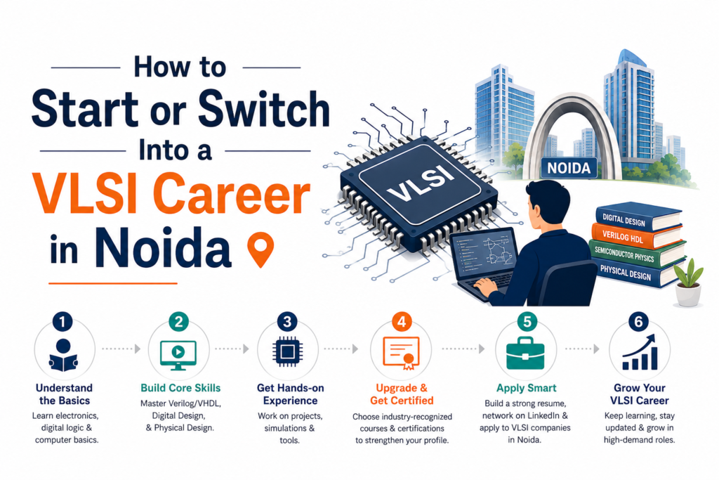
For anyone serious about entering this field, the good news is that you no longer need to relocate to a traditional semiconductor city to get started. A well-structured VLSI course in Noida can now provide the same depth of training — covering RTL design, verification, physical design, and DFT — that was once only available in a handful of southern Indian cities. Many of these programs are built around real, hands-on access to industry-standard EDA tools rather than just theoretical instruction, which matters enormously when it comes to actually landing interviews.
The most effective path tends to combine a focused training program with consistent project-building — working through small design and verification exercises that mirror real industry problems. Pairing that with active networking, whether through local tech meetups or online communities focused on chip design, often opens doors that a resume alone won’t. Given how fast this field moves, staying updated on the latest tools, methodologies, and hiring trends is just as important as the initial learning phase. Choosing a good VLSI course in Noida with strong placement support and updated lab access can significantly shorten the gap between learning and actually working on real silicon.
Conclusion
Noida’s transformation into a semiconductor and VLSI career hub is still unfolding, but the direction is unmistakable. Policy support, a growing base of global and domestic employers, and rising compensation are converging to make this one of the more compelling technology career paths available in North India today. For anyone willing to invest in the right skills, the timing couldn’t be better — the demand is real, the opportunities are diverse, and the region’s momentum shows no signs of slowing down.
1. Why is Noida becoming a VLSI career hub?
Noida’s growing semiconductor ecosystem, global chip companies, and expanding R&D centers are creating strong VLSI career opportunities for freshers and professionals.
2. Are VLSI jobs increasing in Noida?
Yes. Rising semiconductor investments and electronics manufacturing are boosting demand for VLSI engineers in Noida across multiple design domains.
3. Which VLSI roles are in demand in Noida?
RTL Design, Design Verification, Physical Design, DFT, Analog Design, and FPGA engineers are among the most sought-after VLSI roles in Noida.
4. Is Noida a good city for VLSI freshers?
Yes. Noida offers quality VLSI training, internships, and growing semiconductor companies, making it a strong choice for fresh graduates.
5. How is the semiconductor industry creating jobs in Noida?
New chip design centers, government support, and global semiconductor investments are driving demand for skilled VLSI professionals in Noida.