
Understanding MOSFET Basics for VLSI Circuit Design

The Metal-Oxide-Semiconductor Field-Effect Transistor (MOSFET) serves as the foundational building block of modern Very Large Scale Integration (VLSI) circuit design. As semiconductor technology scales down into nanometer regimes, mastering how these four-terminal devices switch, amplify, and manage current becomes essential for building complex Integrated Circuits (ICs). In digital VLSI systems, MOSFETs operate primarily as high-speed electronic switches, forming complementary pairs that allow modern microprocessors to execute billions of operations per second with high energy efficiency. Understanding their physical structure, terminal behaviors, and current-voltage characteristics is critical for any engineer designing digital logic gates, memory arrays, or high-performance analog sub-systems.
To build an intuitive grasp of complementary logic design, it is beneficial to explore the distinct operating traits of N-channel vs P-channel MOSFETs, as their combined behavior enables low-power CMOS architecture. Unlike bipolar junction devices, MOSFETs rely on voltage-controlled field effects across an insulated gate structure, making them voltage-driven rather than current-driven. This fundamental characteristic provides extremely high input impedance, drastically reducing static power consumption in complex IC layouts. As VLSI fabrication advances, understanding how gate potential modulates channel conductivity remains central to optimizing speed, power dissipation, and overall circuit area.
Summary Comparison Table
| Attribute / Parameter | Bipolar Junction Transistor (BJT) | Classic Planar MOSFET | Advanced FinFET / GAA MOSFET |
| Control Mechanism | Current-Controlled ($I_B$) | Voltage-Controlled ($V_{GS}$) | Voltage-Controlled ($V_{GS}$) |
| Input Impedance | Low to Moderate | Extremely High ($>10^{12}\ \Omega$) | Extremely High |
| Primary Carrier Type | Bipolar (Majority & Minority) | Unipolar (Majority Carriers) | Unipolar (Majority Carriers) |
| Static Power Dissipation | Higher (Continuous base current) | Near Zero (Ideal) / Minimal Leakage | Ultra-low (Suppressed Leakage) |
| Short-Channel Resistance | Poor at sub-micron scales | Moderate (Prone to SCEs) | Excellent Electrostatic Control |
| Primary VLSI Application | High-speed RF / BiCMOS | Legacy ICs / Power ICs | High-Performance CPUs / GPUs |
Physical Structure and Terminal Characteristics
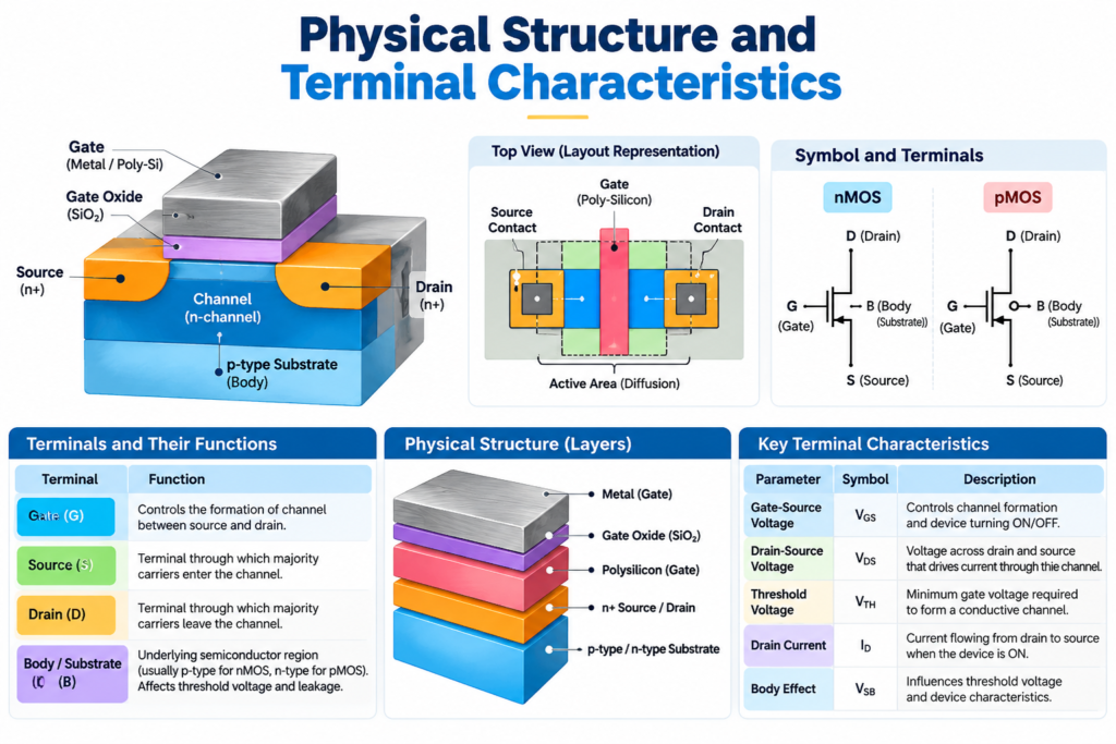
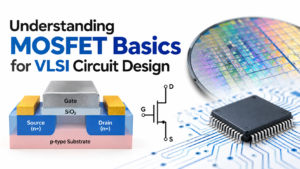
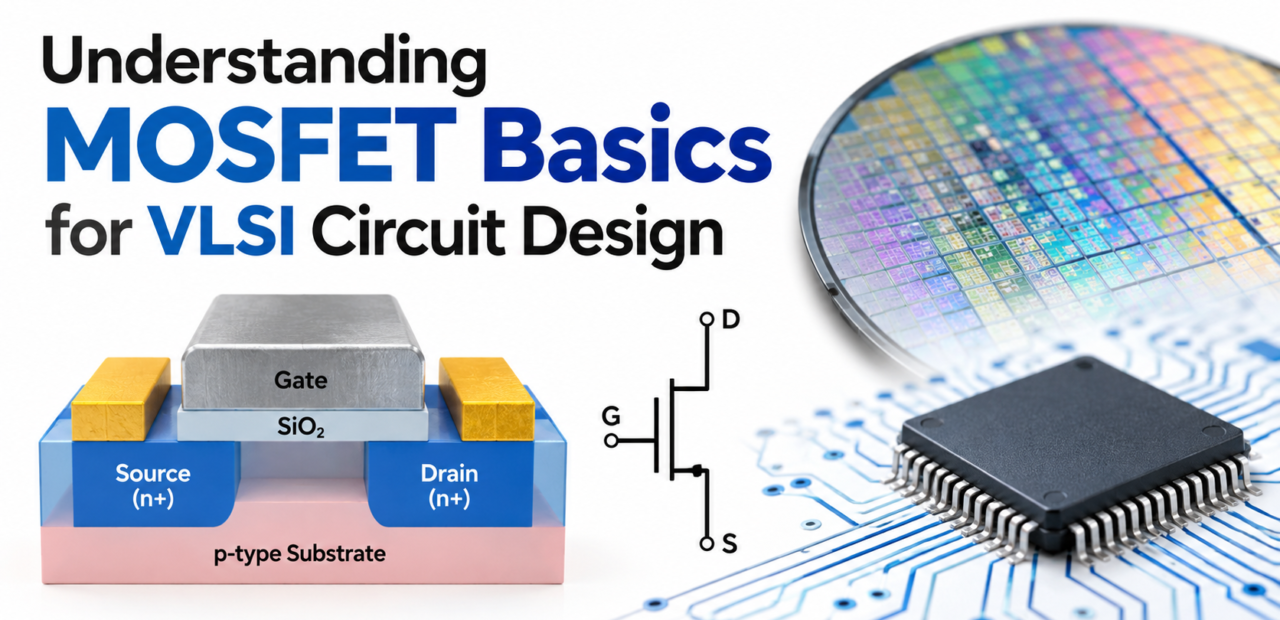
A typical MOSFET is a four-terminal device consisting of the Gate (G), Drain (D), Source (S), and Body or Substrate (B). In planar integrated circuit fabrication, the body is formed on a silicon substrate, while the source and drain regions are heavily doped with opposite polarities to create $p\text{-}n$ junctions. Directly above the channel region between the source and drain lies a thin insulating layer of Silicon Dioxide ($\text{SiO}_2$), topped by a conductive gate electrode made of polysilicon or metal. The gate oxide acts as a dielectric dielectric barrier, preventing direct current flow from the gate into the silicon body under normal DC operating conditions.
During circuit layout, the electrical bias applied across these four terminals controls the distribution of charge carriers within the semiconductor substrate. In an N-channel MOSFET (NMOS), applying a positive voltage to the gate relative to the substrate repels positive holes and attracts free electrons to the surface below the gate oxide. When this gate voltage surpasses a specific threshold voltage ($V_{th}$), a conductive inversion layer forms, physically bridging the source and drain regions. In VLSI cell design, proper body-biasing strategies are frequently employed to control threshold variations and suppress unwanted leakage currents.
Modes of Operation in Integrated Circuits
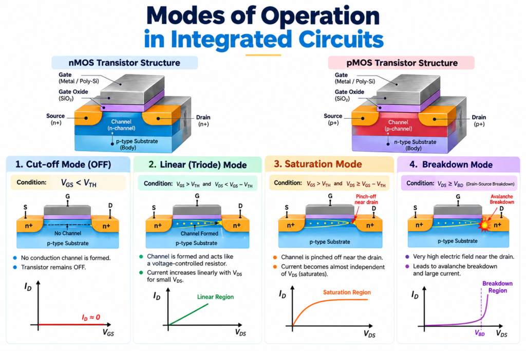
Understanding how field-effect devices function requires analyzing their response to applied voltages compared to conventional bipolar transistors, as explored in detail when studying MOSFET vs Transistor key differences. In integrated circuit design, a MOSFET transitions through three distinct operational regions depending on terminal bias levels: Cut-off, Triode (Linear), and Saturation. In the Cut-off region, the gate-to-source voltage ($V_{GS}$) remains below the threshold voltage ($V_{th}$), keeping the channel non-conductive and restricting current flow between drain and source to negligible subthreshold leakage levels.
When $V_{GS}$ exceeds $V_{th}$ and the drain-to-source voltage ($V_{DS}$) remains low ($V_{DS} < V_{GS} – V_{th}$), the device enters the Triode or Linear region. Here, the conductive inversion layer acts like a voltage-controlled resistor, allowing the drain current ($I_D$) to scale almost linearly with $V_{DS}$. As $V_{DS}$ increases further such that $V_{DS} \ge V_{GS} – V_{th}$, the channel pinches off near the drain end, driving the transistor into the Saturation region. In saturation, $I_D$ becomes largely independent of $V_{DS}$, providing the constant-current characteristics vital for analog amplification and stable digital switching thresholds.
Short-Channel Effects in Deep-Submicron VLSI
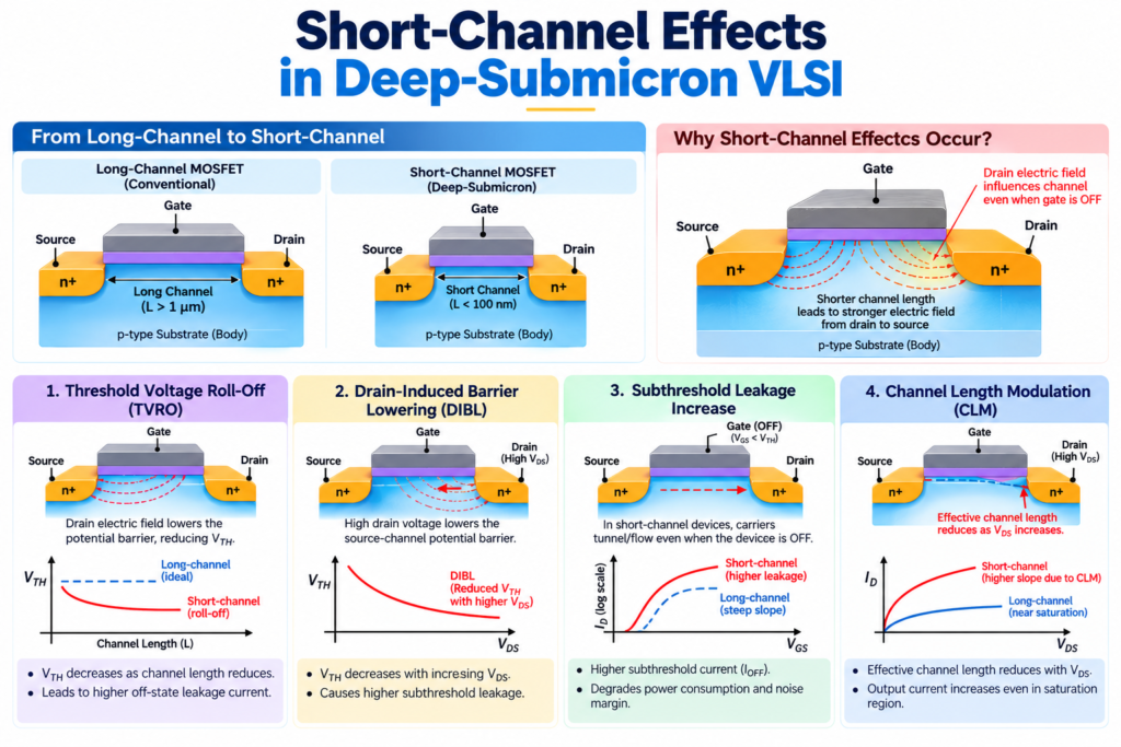
As VLSI manufacturing scales transistor channel lengths ($L$) down into deep-submicron and nanometer dimensions, classic long-channel MOSFET behavior deviates significantly due to short-channel effects (SCEs). When the channel length approaches the physical depletion widths of the source and drain junctions, the gate electrode loses partial electrostatic control over the channel. Consequently, short-channel devices experience unwanted phenomena such as Drain-Induced Barrier Lowering (DIBL), where a high drain voltage lowers the potential barrier at the source edge, reducing the effective threshold voltage and increasing off-state leakage current.
Another critical short-channel challenge is velocity saturation, which occurs when high lateral electric fields cause charge carrier drift velocity to cap out at a physical maximum before reaching theoretical saturation. Additional sub-micron non-idealities include mobility degradation from increased vertical electric fields, hot-carrier injection damaging the gate dielectric, and severe subthreshold conduction. To counteract these short-channel effects in modern VLSI nodes, process engineers have introduced advanced device architectures like FinFETs, Gate-All-Around (GAA) nanosheets, strained silicon channels, and ultra-thin high-$\kappa$ metal gate (HKMG) dielectrics.
MOSFET Applications in Digital and Analog Logic

In digital VLSI system implementation, the complementary combination of NMOS and PMOS transistors forms the cornerstone of Complementary Metal-Oxide-Semiconductor (CMOS) logic design. CMOS technology achieves exceptionally low static power dissipation because, in any stable logic state, either the pull-up PMOS network or the pull-down NMOS network is turned off, preventing direct current flow from power rails ($V_{DD}$) to ground. Standard digital libraries rely on these complementary pairs to construct high-density logic gates, flip-flops, multiplexers, dynamic RAM cells, and static RAM (SRAM) memory cells.
Beyond digital logic, MOSFETs play a crucial role in precision analog and mixed-signal integrated circuit design. Operating primarily in the saturation region, MOSFETs function as high-gain transconductors in operational amplifiers (op-amps), active loads, precision current mirrors, voltage references, and radio-frequency (RF) switches. Balancing channel length, gate width ($W/L$ ratios), noise performance, matching accuracy, and parasitic layout capacitances allows analog designers to meet tight gain, bandwidth, and dynamic range specifications on monolithic silicon dies.
Key Advantages and Scalability Challenges

The primary advantage that enabled MOSFETs to dominate modern electronics is their continuous scalability according to Dennard Scaling principles and Moore’s Law. Because the gate terminal is electrostatically isolated from the channel by a dielectric layer, switching requires negligible continuous input current, allowing billions of devices to be integrated onto a single microchip without immediate thermal failure. Furthermore, the symmetrical physical structure of MOSFETs enables bilateral current flow, providing immense flexibility when designing pass-transistor logic, transmission gates, and complex switching matrices.
Despite these advantages, continued dimensional scaling presents severe engineering challenges at sub-3nm nodes. Excessive quantum tunneling through ultra-thin gate oxides increases gate leakage currents, while high power densities demand complex thermal management solutions. Additionally, process-voltage-temperature (PVT) variations lead to threshold voltage mismatch across adjacent transistors on the same die. Overcoming these barriers requires novel multi-gate device topologies, low-resistance interconnect materials, advanced lithography techniques, and strict design-for-manufacturability (DFM) rules in modern EDA design flows.
Conclusion
MOSFETs remain the undeniable heart of Very Large Scale Integration (VLSI) circuit engineering, enabling the high-density microprocessors, memories, and system-on-chip (SoC) architectures driving modern technology. By leveraging voltage-controlled channel formation across insulated gate structures, designers can achieve high switching speeds alongside minimal static power consumption. While physical scaling challenges like short-channel effects, gate leakage, and manufacturing variations present ongoing hurdles, innovative multi-gate architectures such as FinFETs and GAA nanosheets ensure that MOSFET fundamentals will continue to power next-generation integrated circuits.
What is the fundamental role of a MOSFET in VLSI circuit design?
In VLSI design, a MOSFET acts as a voltage-controlled electronic switch or amplifier. Its ability to turn on or off based on gate voltage allows engineers to integrate billions of complementary logic gates onto a single chip with minimal power consumption.
Why are MOSFETs preferred over BJTs in digital VLSI chips?
MOSFETs possess an insulated gate terminal that provides extremely high input impedance. This means they consume virtually no static DC gate current when turned on or off, whereas BJTs require continuous base current, causing excessive power dissipation in ultra-dense digital chips.
What is threshold voltage ($V_{th}$) in a MOSFET?
Threshold voltage ($V_{th}$) is the minimum gate-to-source voltage ($V_{GS}$) required to create a conductive inversion layer (channel) beneath the gate oxide, allowing current to flow between the drain and source terminals.
What happens when a MOSFET operates in the saturation region?
In saturation, the drain-to-source voltage ($V_{DS}$) is high enough to pinch off the channel near the drain terminal. As a result, the drain current ($I_D$) becomes relatively independent of $V_{DS}$ and is controlled almost entirely by $V_{GS}$, making it ideal for analog amplification.
What are Short-Channel Effects (SCEs) in modern integrated circuits?
Short-channel effects occur when a transistor’s channel length is reduced to nanometer scales. Phenomena like Drain-Induced Barrier Lowering (DIBL), subthreshold leakage, and velocity saturation reduce the gate’s electrostatic control over the channel, degrading device performance.
How does CMOS logic minimize static power consumption?
CMOS logic pairs NMOS and PMOS transistors in a complementary configuration. In any steady logic state (high or low), one network is active while the other is completely turned off, preventing a direct DC current path between the supply rail ($V_{DD}$) and ground.
How do FinFETs and GAA transistors improve upon traditional planar MOSFETs?
FinFETs and Gate-All-Around (GAA) nanosheets wrap the conductive gate electrode around three or four sides of the silicon channel rather than just a single flat surface. This multi-gate geometry drastically improves electrostatic control, mitigates short-channel effects, and reduces off-state leakage current in deep-submicron nodes.