


The Companies Building the Equipment Behind the Semiconductor Industry

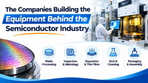
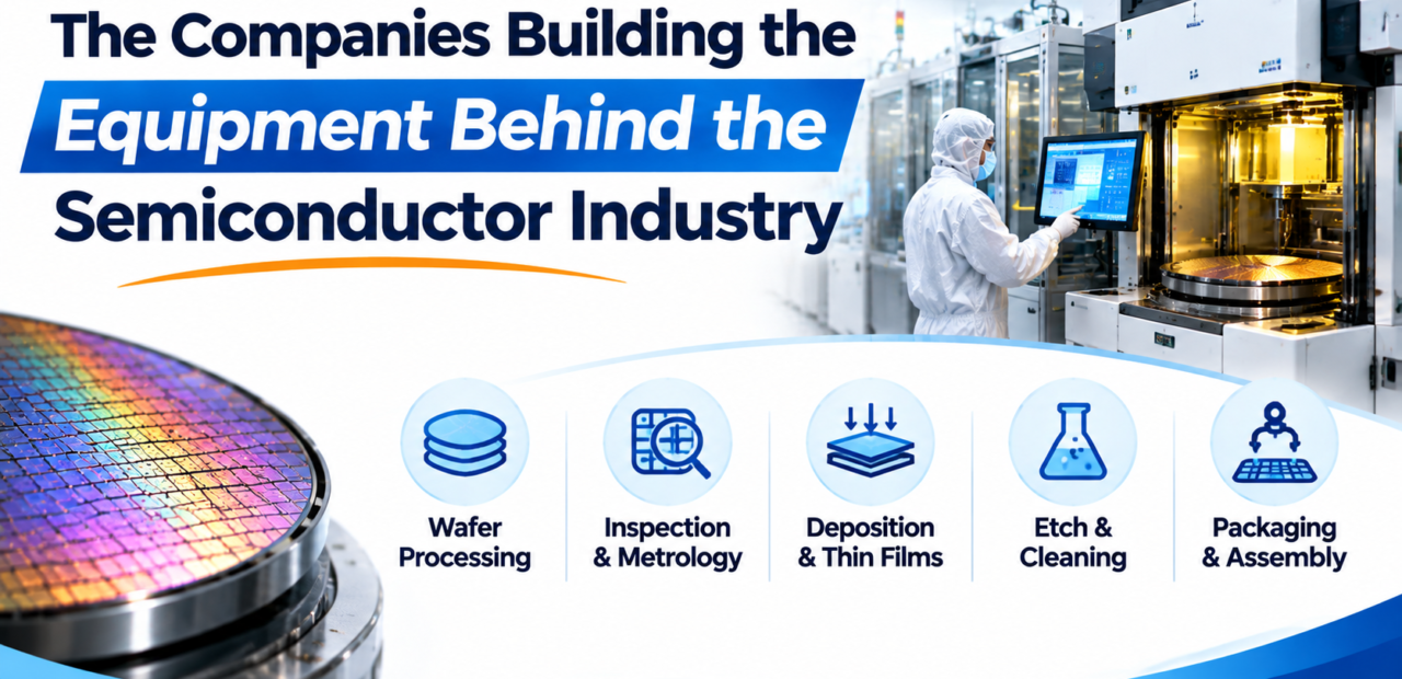
When people discuss the semiconductor industry, attention often goes towards companies designing processors, developing GPUs or manufacturing advanced chips. However, behind every modern semiconductor is another important industry that makes chip production possible: semiconductor manufacturing equipment. These specialised machines are responsible for printing microscopic circuit patterns, depositing thin material layers, removing unwanted materials, inspecting wafers and testing finished chips. Without this equipment, manufacturers would struggle to produce the advanced processors used in smartphones, data centres, automobiles and artificial intelligence systems. As semiconductor technology continues to advance, the companies developing these machines are becoming increasingly important to the global electronics ecosystem.
The demand for advanced semiconductor equipment is growing alongside developments in artificial intelligence, high-performance computing, automotive electronics and next-generation memory technologies. Manufacturing smaller and more powerful chips requires increasingly sophisticated production processes, precise measurements and advanced fabrication tools. Companies such as ASML, Applied Materials, Lam Research, Tokyo Electron and KLA play important roles in supporting these requirements. Their technologies help semiconductor manufacturers improve production accuracy, increase manufacturing efficiency and develop increasingly complex chip architectures. Although these equipment suppliers may operate behind the scenes, their innovations directly influence how quickly the semiconductor industry can advance.
ASML: Advancing Semiconductor Lithography Technology
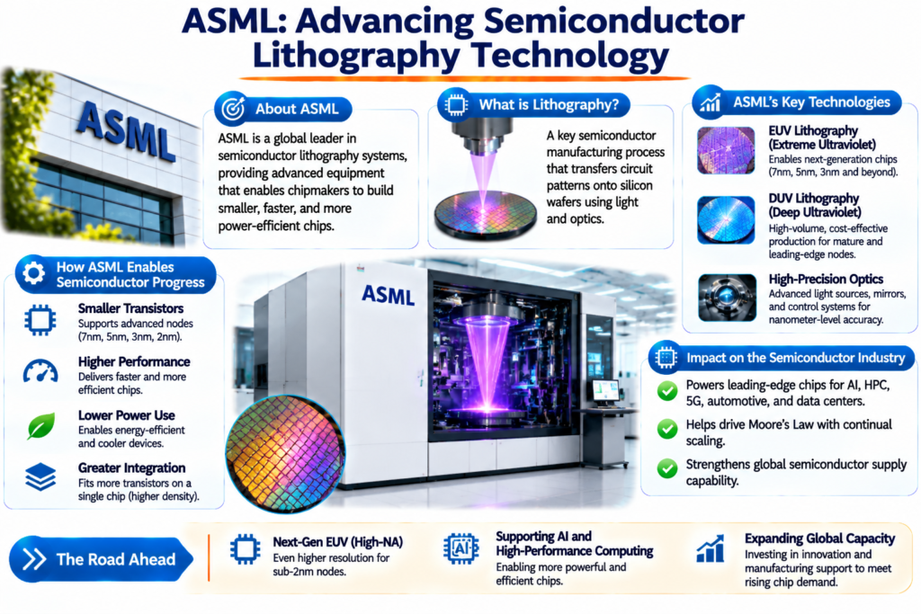
ASML, headquartered in the Netherlands, is one of the most important companies in the semiconductor equipment industry. It develops advanced lithography systems that semiconductor manufacturers use to transfer extremely small circuit patterns onto silicon wafers. Its extreme ultraviolet (EUV) lithography technology enables the production of advanced chip structures that are difficult to achieve using conventional manufacturing methods. ASML is currently the only supplier of EUV lithography systems, making its technology particularly significant for leading-edge semiconductor production.
As chip manufacturers continue developing more advanced processors, lithography equipment becomes increasingly important. ASML’s systems help manufacturers print increasingly complex circuit patterns with high precision. Its technology supports the production roadmaps of major semiconductor manufacturers and contributes to advancements in computing performance, power efficiency and transistor density. The company’s equipment also demonstrates how specialised engineering and continuous research influence the future of semiconductor manufacturing.
Applied Materials: Supporting Multiple Chip Manufacturing Processes
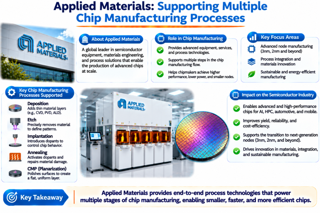
Applied Materials, based in the United States, develops equipment and technologies used across several stages of semiconductor manufacturing. Its portfolio includes deposition, etching, ion implantation, chemical mechanical planarisation and other wafer-processing technologies. These processes help manufacturers build the complex structures that form modern integrated circuits. Rather than focusing on only one manufacturing stage, the company provides a broad range of solutions that support different parts of the wafer fabrication process.
As semiconductor devices become more complex, manufacturers need greater control over material properties, surface quality and microscopic structures. Applied Materials develops technologies that help address these requirements while supporting improvements in manufacturing productivity and process performance. Its equipment is used in the production of logic chips, memory devices and other semiconductor components. This broad presence makes the company an important technology partner for semiconductor manufacturers worldwide.
Lam Research: Developing Advanced Etching and Deposition Equipment
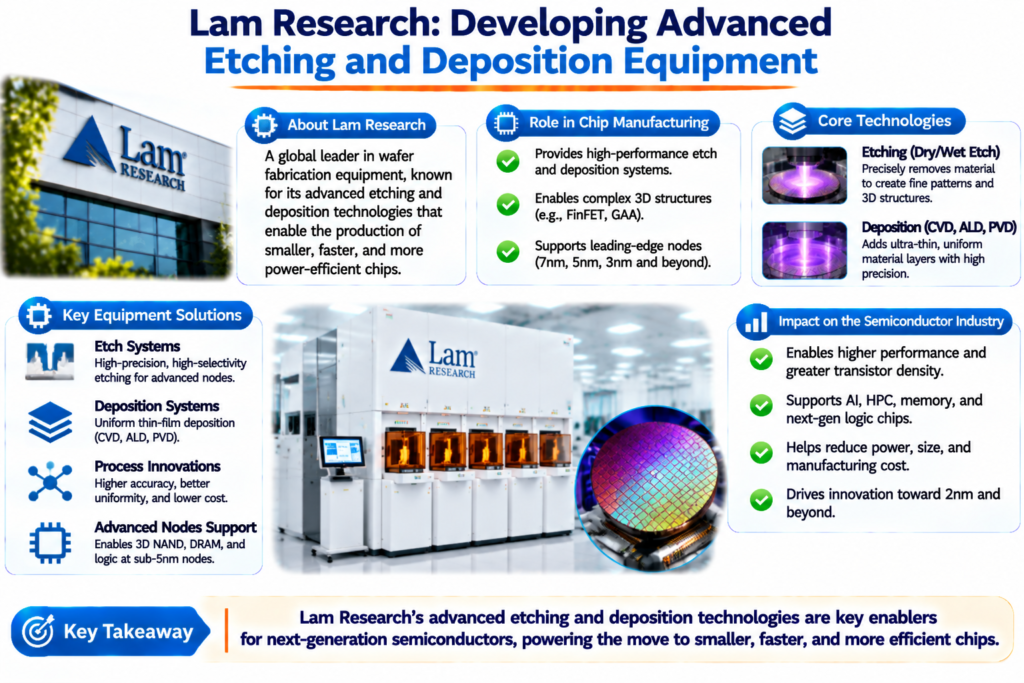
Lam Research is another major semiconductor equipment manufacturer headquartered in the United States. The company specialises in technologies such as plasma etching, thin-film deposition and wafer cleaning. These processes are essential for creating the detailed structures found inside semiconductor devices. Etching removes selected material from a wafer, while deposition adds controlled layers that form insulating and conducting structures.
The growing complexity of memory and logic devices has increased the importance of precise etching and deposition technologies. Advanced memory architectures, including 3D NAND, require manufacturers to create structures with increasingly demanding geometries. Lam Research develops equipment designed to support these manufacturing challenges. Its technologies help semiconductor manufacturers control critical dimensions, improve process consistency and develop advanced device architectures.
Tokyo Electron: Strengthening Wafer Processing and Cleaning Technologies
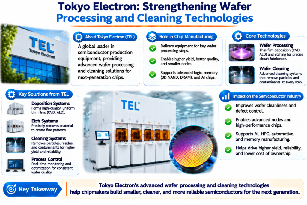
Tokyo Electron, headquartered in Japan, is a major supplier of semiconductor production equipment. Its technologies support several important manufacturing processes, including deposition, coating and developing, etching and wafer cleaning. These processes help prepare silicon wafers and create the material structures required for semiconductor devices. The company’s equipment is used by manufacturers producing a wide range of semiconductor products.
One important area of semiconductor manufacturing is wafer cleaning, where unwanted particles and chemical residues must be removed to maintain production quality. Even extremely small contaminants can affect device performance and manufacturing yields. Tokyo Electron develops specialised equipment to support precise wafer processing and cleaner manufacturing environments. Its technologies contribute to the consistency and reliability required in advanced semiconductor fabrication facilities.
KLA: Improving Semiconductor Inspection and Process Control
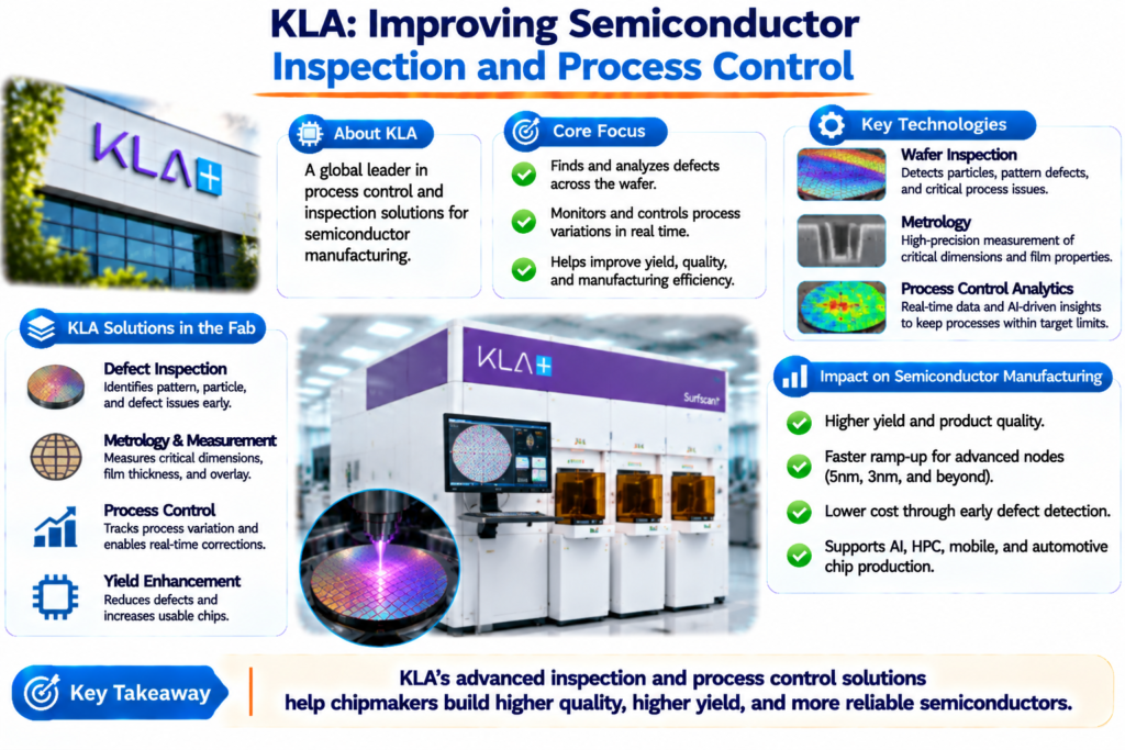
KLA, based in the United States, focuses on inspection, metrology and process-control technologies. Semiconductor manufacturing involves hundreds of complex processing steps, and defects can occur during different stages of production. KLA develops systems that help manufacturers detect defects, measure microscopic structures and monitor process variations. These capabilities are essential for maintaining production quality as semiconductor devices become smaller and more complex.
Inspection and measurement are particularly important because a manufacturing defect can affect the performance or reliability of an entire chip. KLA’s technologies provide semiconductor manufacturers with information that helps identify production problems and improve manufacturing processes. Its solutions support yield management, quality control and process optimisation. As advanced packaging and next-generation chip architectures develop, inspection and measurement technologies will remain important parts of the semiconductor manufacturing ecosystem.