



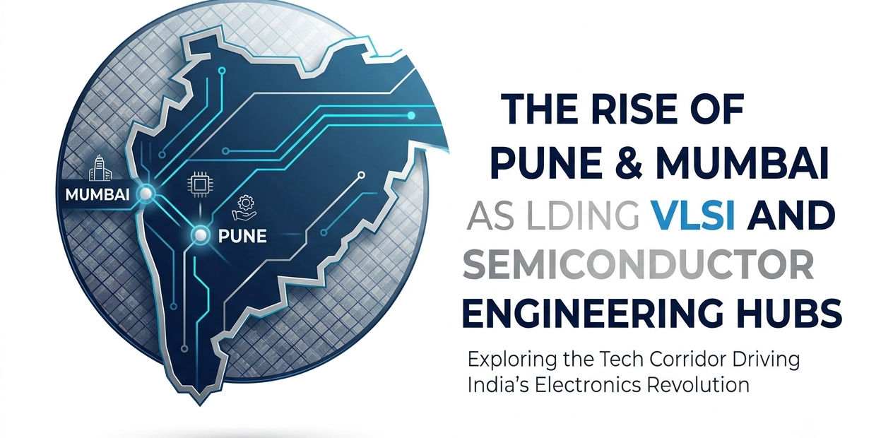
The Rise of Pune and Mumbai as Leading VLSI and Semiconductor Engineering Hubs

A decade ago, nobody would have named Pune or Mumbai in the same breath as global chip design. Today, both cities sit at the centre of India’s most ambitious industrial bet — building the silicon that powers everything from smartphones to electric vehicles.
This shift didn’t happen overnight. It came from years of quiet groundwork: engineering talent that stayed and grew, government policy that finally caught up with intent, and global companies deciding India’s western belt was ready for serious semiconductor work. Here’s how Pune and Mumbai got here, and what it means for the region’s future.
From Software City to Silicon City: Pune’s VLSI Transformation
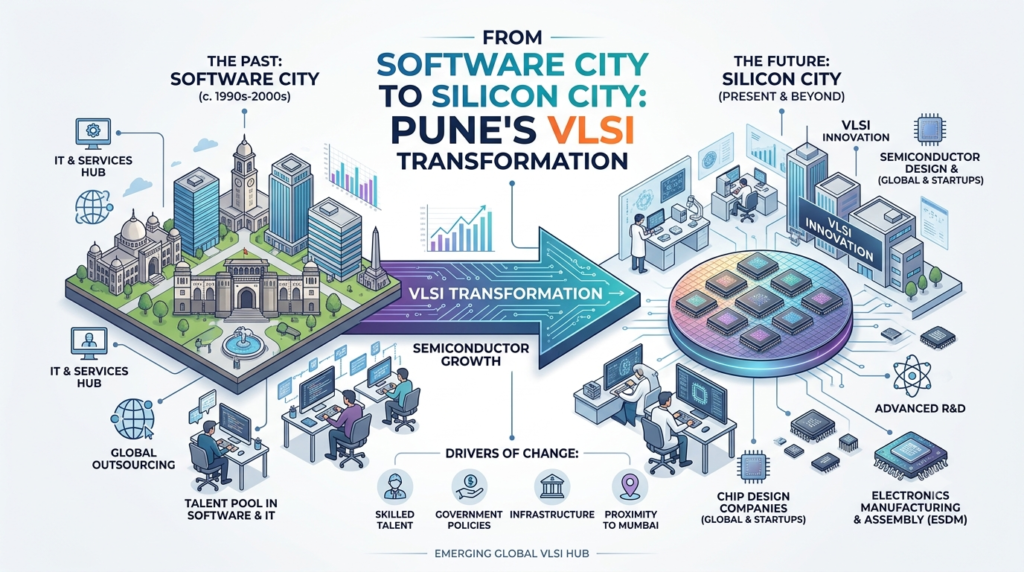
Pune built its early reputation on IT services and automotive manufacturing, but over the past few years, it has quietly transformed into a genuine VLSI design hub. Global chipmakers such as Intel, NXP, and Qualcomm now run full-fledged design operations out of the city, covering everything from RTL design to physical design and verification. Around these multinational teams, a layer of smaller VLSI service companies has grown as well, creating a diverse, multi-tiered ecosystem rather than one dominated by a single employer.
The clearest signal of this shift came in January 2026, when Pune hosted the 39th VLSI Design & Embedded Systems Conference — one of the most closely watched semiconductor events in the country. Industry leaders used the platform to push India toward a “product-led” strategy: building complete electronic products and owning domestic intellectual property, rather than functioning solely as a design-and-manufacturing back office for foreign companies. The fact that this conversation happened in Pune, rather than being imported from elsewhere, reflects how significantly the city’s standing in the semiconductor world has changed.
Bharat Electronics Limited (BEL) added further momentum by opening a new fabrication facility in Pune in mid-2026, partnering with the Semi-Conductor Laboratory to co-develop integrated circuits for defence-grade applications. It’s a modest facility by global standards, but symbolically significant — it puts actual chip fabrication, not just design work, on Pune’s map.
This growing ecosystem has also created real demand for skilled talent, which is why more engineers and students are turning to online VLSI training in Pune to build the practical, industry-ready skills these design centres are actively hiring for.
Mumbai’s Entry Point: Capital, Infrastructure, and a New Industrial Identity
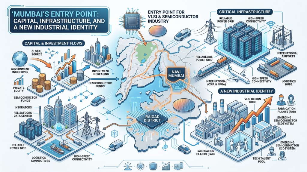
Mumbai’s semiconductor story looks quite different from Pune’s. Rather than growing organically around design talent, Mumbai’s entry into the sector has been driven largely by capital and infrastructure investment. Navi Mumbai now hosts Maharashtra’s first semiconductor OSAT (assembly, testing, and packaging) plant, developed by the RRP Group in phases, with cumulative state investment running into tens of thousands of crores of rupees. It was a deliberate move by the state government to plant a manufacturing anchor near India’s financial capital, rather than leaving semiconductor development entirely to Gujarat, Karnataka, or Tamil Nadu.
Reliance Industries has added further weight to the region’s ambitions, with plans for a large-scale industrial and data-centre ecosystem around Navi Mumbai that ties together logistics, power, and electronics manufacturing. None of this makes Mumbai a design hub in the way Pune is — the city’s real strength lies in finance, infrastructure, and large-scale project execution — but it gives Maharashtra a second, complementary node in the semiconductor value chain: one city designing chips, another helping package, test, and move them.
As this manufacturing ecosystem takes shape, the city is also seeing rising interest from engineers and students exploring a VLSI course in Mumbai, drawn by the packaging, testing, and infrastructure-side career opportunities emerging alongside these large-scale investments.
Government Push: Maharashtra’s Incentive Framework and the India Semiconductor Mission
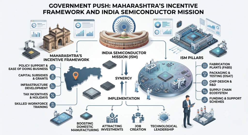
None of this growth happened without deliberate policy support. At VLSID 2026, VLSI Society of India president Satya Gupta made a pointed argument: Maharashtra could close its gap with more established semiconductor states by funding up to 25 to 26 percent of project costs across product development and manufacturing, while also investing in engineering and technician-level training. He noted that electronics and semiconductors already contribute close to 37.5 percent of India’s GDP, a figure expected to cross 50 percent by 2047 — numbers that explain why state governments are competing hard for this industry.
At the national level, the India Semiconductor Mission has committed well over ₹76,000 crore toward the broader ecosystem, covering chip design incentives, fabrication partnerships, and OSAT facilities. The Union Budget for 2026-27 allocated its largest-ever single-year outlay to the mission, reflecting how central semiconductors have become to India’s industrial policy rather than a niche technology bet. Maharashtra, with Pune’s design talent and Mumbai’s capital and logistics strength, is positioning itself to capture a meaningful share of that national push.
Major Companies and Projects Driving the Region’s Growth
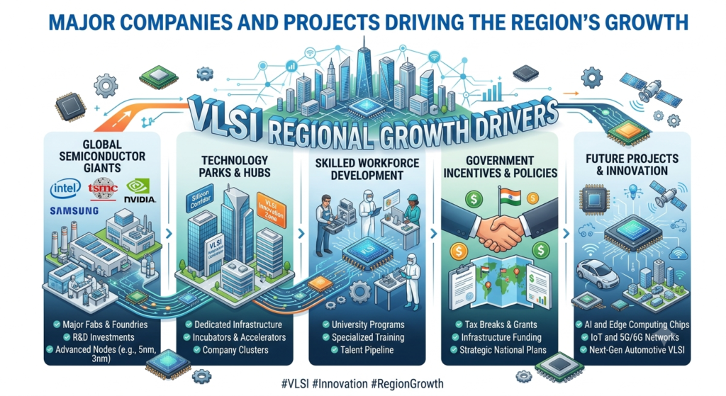
The list of organisations active in the Pune-Mumbai corridor has grown well beyond the usual multinational names. TCS used VLSID 2026 to showcase work on chiplet-based multi-die systems, RISC-V processor development, and AI-assisted chip design tools — signalling that Indian IT majors are moving from services support into genuine semiconductor engineering. HCL Technologies has expanded its own semiconductor engineering footprint with new design centres, while RRP Electronics and Suchi Semicon are among the first companies setting up OSAT facilities in Maharashtra ahead of central government subsidy approvals.
This mix matters. It’s not just global chip giants parachuting into India; it’s a combination of multinational R&D centres, homegrown IT companies pivoting into hardware, state-backed manufacturing ventures, and specialised design service firms — all operating in overlapping geography. That density is what turns a city into an ecosystem rather than just a location with a few large offices.
What This Means for Engineering Careers and Jobs in the Region
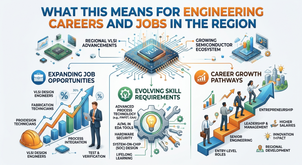
For engineers already working in chip design or looking to move into it, the practical impact of this growth is significant. Pune now ranks consistently among India’s top cities for VLSI hiring, alongside Bengaluru, Hyderabad, and Noida, with roles spanning RTL design, verification, physical design, and analog layout. Industry estimates suggest India will need tens of thousands of additional VLSI engineers over the next few years, and salaries in specialised areas — advanced-node physical design, verification with strong coverage-closure experience, and mixed-signal layout — have been rising well above general IT pay scales.
Mumbai’s growth adds a different kind of opportunity: roles in manufacturing operations, quality and testing, supply chain, and plant engineering around the new OSAT and packaging facilities, rather than pure design work. Together, the two cities offer a fuller career pipeline within a single region — design-heavy roles in Pune, operations and manufacturing-linked roles in and around Mumbai — something few other parts of India currently offer in combination.
Conclusion
Neither city is going to overtake Bengaluru as India’s semiconductor design capital in the near term, and neither is likely to match Gujarat’s scale in fabrication. But that isn’t really the point. Pune and Mumbai are carving out a distinct role: a design and engineering hub paired with a manufacturing and capital hub, both backed by an unusually active state government. For a region that had no real presence in this industry a decade ago, that combination is a genuine structural shift — and one that’s still early enough for engineers, companies, and policymakers to shape what comes next.
Why are Pune and Mumbai becoming VLSI hubs?
Pune and Mumbai are emerging VLSI hubs due to semiconductor investments, skilled engineers, strong IT ecosystems, and growing demand for chip design talent.
Is Pune good for a VLSI career?
Yes. Pune offers growing opportunities in VLSI design, semiconductor engineering, embedded systems, verification, and electronics manufacturing.
Is Mumbai a good city for semiconductor jobs?
Mumbai is developing as a semiconductor and electronics hub, offering opportunities across chip design, engineering services, and technology companies.
Why choose Pune for VLSI training?
Pune provides access to VLSI training institutes, engineering talent, technology companies, and practical career opportunities for aspiring semiconductor engineers.
What VLSI jobs are available in Pune and Mumbai?
Popular roles include RTL Design Engineer, Verification Engineer, Physical Design Engineer, DFT Engineer, Analog Designer, and Semiconductor Engineer.