



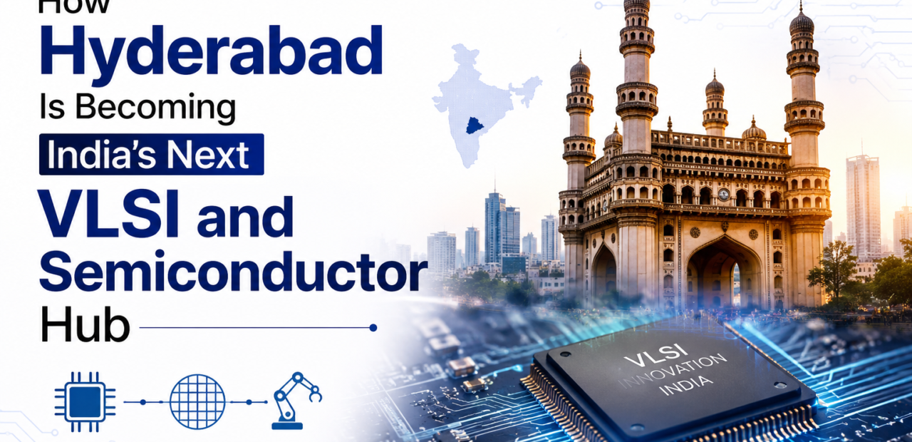
How Hyderabad Is Becoming India’s Next VLSI and Semiconductor Hub

A decade ago, if you asked someone where India’s chip design action was happening, the answer was almost always Bengaluru. That’s changing fast, and the city rewriting the script is Hyderabad.
Global chip giants have quietly built massive design centers here, homegrown startups are working on everything from AI processors to RISC-V cores, and the state government is pushing policies that make it easier for the semiconductor ecosystem to grow. What was once seen as a strong IT city is now being talked about in the same breath as global chip design hotspots. This shift didn’t happen overnight, and understanding how it unfolded tells you a lot about where the industry is headed next.
1. A Talent Base That Has Been Building for Years

Hyderabad’s rise isn’t a sudden trend — it’s the result of years of quiet groundwork. The city already hosts several of the world’s top semiconductor firms, and its chip design workforce has grown steadily, now numbering in the thousands and expanding every year. This pool of design talent covers everything from RTL design and verification to physical design and chip architecture.
What makes this pool valuable is depth, not just size. Engineers here have worked across multiple product generations, giving the city an institutional memory that’s hard to replicate elsewhere. Global companies notice this. When a firm is deciding where to expand its design operations, a mature, experienced workforce is often the deciding factor over a location that’s simply cheaper. This is also why the demand for a good VLSI institute in Hyderabad has grown so sharply — companies need a steady pipeline of trained engineers to keep up with expansion plans, and existing training centers are working to fill that gap.
2. Government Policy and Infrastructure Push

Telangana’s state government has been active in courting semiconductor investment, offering incentives, dedicated land parcels, and faster clearances for companies setting up design and R&D centers. This is happening alongside a broader national push — India’s semiconductor mission has approved a growing number of design and manufacturing projects across the country, with policy support aimed at building a self-reliant chip ecosystem.
Hyderabad has been positioned as a key player in this national roadmap, with semiconductor design specifically called out as one of the priority areas for the city. Manufacturing-heavy states like Gujarat and Assam are pulling ahead in fabrication plants, but design work — the part of the value chain that pays the best and requires the deepest technical skill — is where Hyderabad is carving out its lead. This distinction matters because design roles tend to be more stable and higher-paying compared to manufacturing-floor jobs.
3. A Growing Startup and Innovation Ecosystem

It isn’t just multinational giants driving this growth. Hyderabad now has a genuine cluster of homegrown semiconductor startups working on domain-specific chips, AI accelerators, and IP cores for automotive and telecom use cases. Several of these companies have received support under national design-linked incentive programs, giving them access to funding, tools, and infrastructure that used to be out of reach for smaller players.
This startup layer is important because it diversifies the kind of work available in the city. Instead of every opportunity being tied to a large multinational, engineers now have a choice between established corporate design centers and smaller, faster-moving startups experimenting with newer architectures like RISC-V. That variety keeps the ecosystem healthy and gives the city a more resilient, well-rounded chip design economy rather than one dependent on a handful of large employers.
4. Why the Job Market Is Heating Up

This brings us to the part most people actually care about — the jobs. With so many companies expanding their design footprints in the city, the result is straightforward: VLSI engineers are in high demand in the market, and that demand shows no signs of slowing down.
A few things are driving this surge. First, chip design work has become far more complex — modern processors pack in AI capability, power efficiency, and security features that require specialized skills across RTL design, verification, physical design, and DFT (design for test). Second, as older engineers move into senior architecture and leadership roles, there’s a widening gap at the mid and entry levels that companies are racing to fill. Third, the shift toward domestic chip design under India’s self-reliance push means more projects are being run locally instead of being outsourced, which directly translates into more local hiring.
For anyone building a career in this space, this is arguably the best time in years to get in. Salaries for skilled VLSI engineers have climbed noticeably, and companies are increasingly willing to invest in training candidates who show strong fundamentals, even if their prior work experience is limited. This is another reason a solid VLSI institute in Hyderabad has become such a valuable stepping stone — it bridges the gap between theoretical knowledge and the kind of hands-on, tool-based skills that hiring managers actually screen for.
It also helps that the roles themselves have diversified. A few years ago, most openings clustered around RTL design and functional verification. Today, the range is much wider — physical design, static timing analysis, DFT, analog layout, and even chip-level architecture roles are all seeing steady openings. This spread means there’s room for people with different strengths and interests to find a lane that suits them, rather than everyone competing for the same narrow set of positions.
Common Roles Driving This Demand
To put the demand in perspective, here’s a quick look at the kind of profiles companies in Hyderabad are actively hiring for right now:
- RTL Design Engineers — building the logic that defines how a chip behaves
- Verification Engineers — testing chip designs before they go to fabrication
- Physical Design Engineers — turning a logical design into a manufacturable layout
- DFT Engineers — ensuring chips can be tested efficiently once produced
- Analog and Mixed-Signal Designers — a smaller but highly specialized and well-paid niche
Each of these paths has its own learning curve, and the right training path can look quite different depending on which one someone is aiming for.
5. What This Means for the City’s Future

Where does this leave Hyderabad five or ten years from now? If current momentum holds, the city is positioned to become one of the anchor points in India’s broader plan to build a chip ecosystem worth well over a hundred billion dollars by the mid-2030s. That’s not a small ambition, and it isn’t guaranteed — global competition in chip design is intense, and cities like Bengaluru and Chennai aren’t standing still either.
But Hyderabad has a few structural advantages working in its favor: a deep and experienced talent base, active government backing, a growing startup layer, and an increasingly diverse mix of employers ranging from global giants to nimble local companies. Add to that the city’s existing strengths in embedded systems and chip verification, and it’s easy to see why analysts keep pointing to Hyderabad as a city to watch.
For engineers and career-changers looking at the semiconductor space, the takeaway is simple: the opportunities in Hyderabad aren’t a passing trend tied to one company or one policy announcement. They reflect a broader, structural shift in where chip design work is happening in India — and that shift is still in its early innings.
Conclusion
Hyderabad’s transformation into a semiconductor and VLSI powerhouse has been years in the making, and it’s now reaching a point where the momentum is hard to ignore. Between strong government support, an expanding startup scene, and a talent pool that keeps growing, the city is quietly building the kind of ecosystem that other regions will be studying for years to come.
If you’re considering a career in this field, now is a good time to pay attention — the demand is real, the opportunities are diverse, and Hyderabad is right at the center of it.
1. Why is Hyderabad becoming a VLSI hub in India?
Hyderabad is attracting global semiconductor companies, chip design centers, and government investments, making it one of India’s fastest-growing VLSI hubs.
2. Is Hyderabad good for VLSI jobs?
Yes. Hyderabad offers excellent VLSI opportunities in RTL Design, Verification, Physical Design, DFT, and Analog with leading semiconductor companies
3. Which VLSI companies are in Hyderabad?
Hyderabad hosts companies like Qualcomm, AMD, NVIDIA, Micron, Synopsys, Cadence, Intel, and other global semiconductor firms.
4. Why are semiconductor companies investing in Hyderabad?
Strong infrastructure, skilled engineers, government support, and a growing semiconductor ecosystem make Hyderabad an attractive investment destination.
5. Is Hyderabad better than Bengaluru for VLSI careers?
Both cities offer excellent VLSI jobs, but Hyderabad is growing rapidly with new semiconductor investments, competitive salaries, and lower living costs.