



Bangalore Is the Best Place for VLSI Training — A Complete Guide

What if the next chip inside your phone, your car, or your smartwatch was designed by someone sitting a few kilometers away from you, right now, in a lab in Bangalore? That’s not a stretch — it’s already happening, every single day, in this city.
If you’ve been searching for the right place to build a career in chip design, you’ve probably noticed one name coming up again and again: Bangalore. It isn’t hype. The city genuinely offers something most other locations in India can’t match when it comes to VLSI training — real proximity to the industry itself. In this guide, we’ll break down exactly why that matters, what to look for in a good training program, how to think about the top 10 VLSI training institutes in Bangalore, and where a career in this field can actually take you.
Why Bangalore Leads India’s VLSI and Semiconductor Ecosystem

Bangalore earned the nickname “Silicon Valley of India” for a reason. It’s home to design centers of nearly every major semiconductor company — from global chip giants to specialized fabless design houses — all operating within a fairly compact radius of the city. That concentration changes everything about how VLSI training in Bangalore actually works.
When a training institute is located a short drive from a dozen chip design offices, the connection between classroom and career shortens dramatically. Trainers are often people who’ve spent years inside these companies. Curriculum updates happen faster because instructors hear directly from hiring teams about what skills are missing in new hires. Guest lectures, internship pipelines, and referral-based hiring all become easier to arrange when the ecosystem is this dense.
There’s also a compounding effect. Because so many engineers already work in VLSI here, the city has built up a strong peer network — online communities, meetups, and alumni groups where people swap interview experiences and job leads. This informal network is often just as valuable as the formal training itself, and it simply doesn’t exist at the same scale anywhere else in the country.
Finally, cost of access matters. Bangalore’s rental and living costs, while not the cheapest in India, are balanced by the sheer number of job openings and the density of opportunities within a small area, so the time-to-employment tends to be shorter compared to cities where the industry presence is thinner.
What to Look for When Choosing VLSI Training in Bangalore
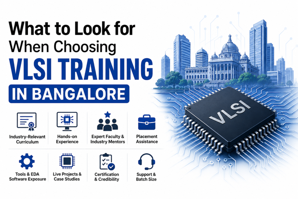
Not every training program delivers the same outcome, and the semiconductor field is specific enough that the wrong choice can cost you months. Before enrolling anywhere, it helps to evaluate a program against a few practical criteria.
Curriculum depth over curriculum breadth. A good program doesn’t try to touch every topic in VLSI superficially. It picks a track — say, physical design, design verification, DFT, analog layout, or FPGA-based design — and goes deep enough that you can actually contribute to a real project on day one of a job.
Hands-on lab time. Theory-heavy courses rarely translate into job readiness in this field. Look for programs where a large share of the schedule is spent inside EDA tools doing real design, simulation, and debugging work, not just watching slides.
Trainer background. Ask directly how many years the instructors have spent working in the industry, and in what roles. Someone who has sat through tape-outs and verification sign-offs teaches very differently than someone who has only taught.
Placement support that’s specific, not vague. “Placement assistance” can mean anything from a genuine referral network to a single resume-review session. Ask for details: how many people from recent batches were placed, in what roles, and at which kinds of companies.
Project portfolio at the end. A strong program leaves you with two or three solid projects you can speak about confidently in an interview — not just a certificate.
Top 10 VLSI Training Institutes in Bangalore: How to Compare Them
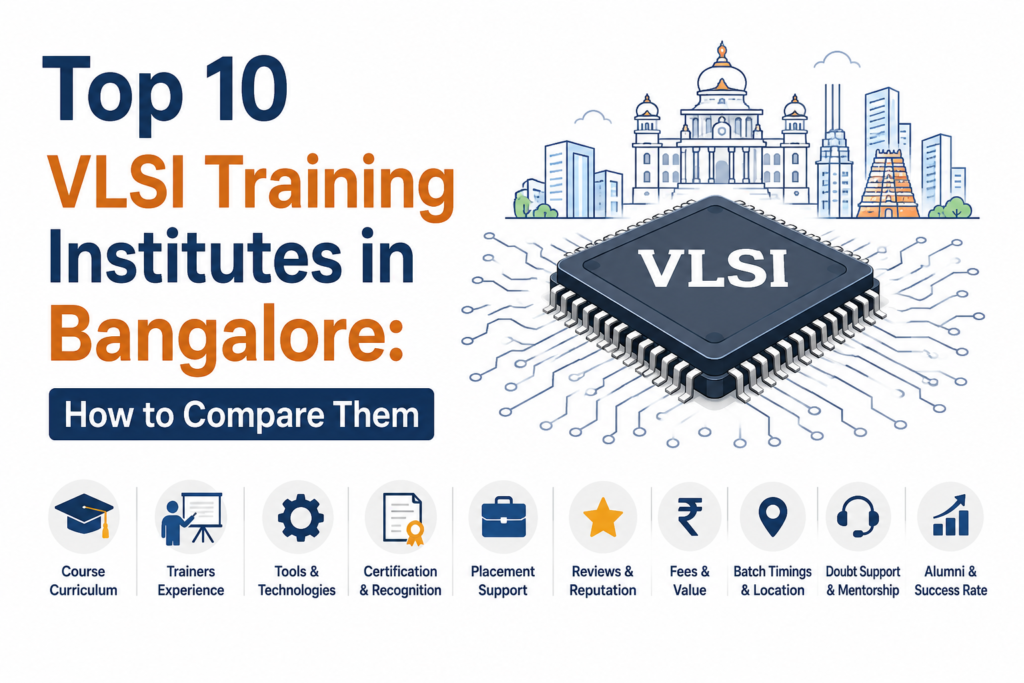
Search for “top 10 VLSI training institutes in Bangalore” and you’ll find dozens of lists, many of them published by the institutes themselves. That doesn’t mean the information is useless — it just means you need a framework for reading between the lines.
Instead of trusting a ranking blindly, build your own shortlist using a simple comparison table with these columns: specialization offered (physical design, verification, DFT, analog, FPGA), course duration, batch size, tool access (industry-standard EDA software versus open-source alternatives), fee structure, and — most importantly — verifiable outcomes from recent batches, not testimonials alone.
A few patterns tend to hold true across the well-regarded names in the city: they keep batch sizes small enough for individual attention, they update their syllabus at least once a year to reflect what companies are actually hiring for, and they’re transparent about which specific job roles their graduates typically land, rather than making broad promises. Visiting the institute in person, sitting in on a demo class, and speaking to two or three recent graduates directly will tell you more than any published “top 10” list ever could.
It’s also worth checking whether an institute has ties to specific companies for internships or direct hiring, since that single detail often has more impact on your first job than any other feature on a brochure.
Career Paths and Job Roles After VLSI Training
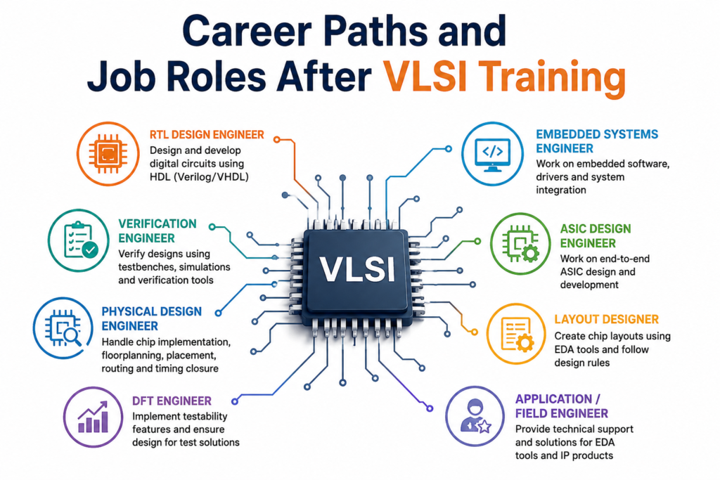
One of the most attractive things about this field is how many distinct career tracks branch out from a single training foundation. Once you’ve built core skills, the paths generally split into a handful of well-defined roles.
Design engineer roles focus on building the actual logic and architecture of a chip — turning specifications into working RTL code.
Verification engineer roles exist to catch every possible flaw before a chip goes to manufacturing, since a mistake caught after fabrication can cost millions. This has become one of the most in-demand tracks in recent years because verification complexity keeps growing faster than design complexity.
Physical design engineer roles take verified logic and turn it into an actual physical layout — placement, routing, timing closure — ready for the foundry.
DFT (Design for Testability) engineer roles focus on making sure chips can be efficiently tested once manufactured, a skill set that’s often underrepresented compared to demand.
Analog and mixed-signal design roles suit people drawn to circuit-level work rather than purely digital logic, and tend to command strong salaries precisely because fewer people specialize in this direction.
Beyond these core tracks, adjacent opportunities exist in FPGA prototyping, embedded systems that interface with custom silicon, and increasingly, roles that blend chip design knowledge with machine learning hardware acceleration — a fast-growing niche as AI workloads push demand for specialized chips.
Latest Trends Shaping VLSI Training and Careers in 2026
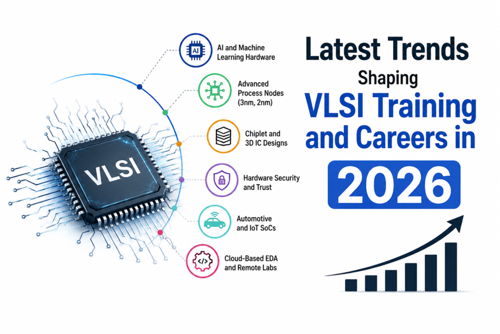
The field isn’t static, and training that ignores current shifts leaves people underprepared. A few trends are worth tracking closely right now.
The global push toward AI-specific chips — accelerators, edge-AI processors, and custom silicon for data centers — has created strong demand for engineers who understand both traditional chip design and the unique constraints of AI hardware. Training programs that have added even a module on this are giving people a real edge.
Government-backed semiconductor manufacturing initiatives in India have also started translating into more design-related hiring locally, rather than just outsourced verification work for overseas teams. This shift means training that covers full design-to-tape-out flow, not just isolated tasks, is becoming more valuable.
Open-source EDA tools are gaining traction as a supplement to expensive commercial licenses, particularly for early practice before moving to industry-standard tools during an internship or job. Programs that expose learners to both environments tend to produce more adaptable engineers.
Finally, hybrid and blended learning formats — a mix of in-person lab access and recorded theory sessions — have become far more common, making it easier for working professionals to reskill into VLSI without quitting a current job outright.
Conclusion
Choosing where to train for a career in chip design isn’t just about picking a course — it’s about picking an ecosystem. Bangalore’s density of design centers, experienced trainers, active peer networks, and evolving industry needs make it one of the strongest launchpads in the country for this field. The real work still comes down to you: comparing programs carefully, insisting on hands-on depth over surface-level coverage, and choosing a path — design, verification, physical design, DFT, or analog — that actually fits how you think and work. Do that well, and Bangalore’s ecosystem does the rest of the heavy lifting for your career.
1. Why is Bangalore the best place for VLSI training?
Bangalore is India’s semiconductor hub, offering top VLSI institutes, experienced mentors, hands-on training, and excellent placement opportunities.
2. Which is the best VLSI training institute in Bangalore?
The best institute offers industry-focused training, Synopsys or Cadence tools, live projects, experienced faculty, and strong placement support.
3. Is Bangalore good for VLSI freshers?
Yes. Bangalore has many semiconductor companies hiring freshers with practical VLSI skills in RTL Design, Verification, Physical Design, and DFT.
4. What is the duration of a VLSI course in Bangalore?
Most VLSI training programs in Bangalore last 3 to 6 months, depending on the specialization and practical project requirements.
5. Which VLSI course has the highest demand?
RTL Design, Design Verification, Physical Design, DFT, and Analog Layout are among the most in-demand VLSI specializations in Bangalore.