



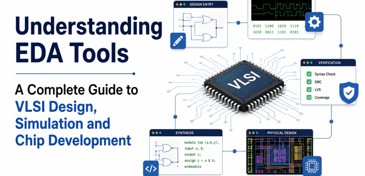
Understanding EDA Tools: A Complete Guide to VLSI Design, Simulation and Chip Development

Somewhere between an idea sketched on a whiteboard and a working chip inside your phone, billions of transistors get placed, wired, tested, and verified without a single human hand touching most of them. That leap from concept to silicon happens because of a category of software most people have never heard of — and it quietly runs the entire modern electronics industry.
That software is known as EDA, short for Electronic Design Automation, and it is the invisible backbone behind every processor, sensor chip, and AI accelerator built today. Whether you’re curious about how chips are actually made or you’re evaluating tools for a design project, this guide breaks down what EDA tools do, how they fit into the chip development process, and what’s changing in the industry right now.
What Are EDA Tools and Why They Matter
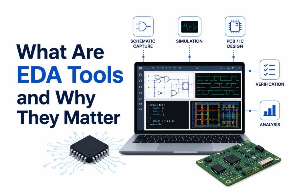
EDA tools for semiconductor design are software applications that let engineers describe, simulate, verify, and physically implement integrated circuits before anything is manufactured. A modern chip can contain tens of billions of transistors, and no design team could place or check that complexity by hand. These tools take a functional description of a circuit, written in a hardware description language, and carry it through simulation, logic synthesis, layout, and final verification.
The value of electronic design automation tools for VLSI isn’t just speed. It’s also accuracy. A single undetected timing error or layout violation can mean a chip fails after fabrication, costing months of schedule and millions of dollars in wasted mask sets. EDA software catches these problems early, models how a design will behave under real electrical, thermal, and mechanical conditions, and gives engineers confidence that the design will work the first time it reaches a fab.
The Main Categories in EDA Tools
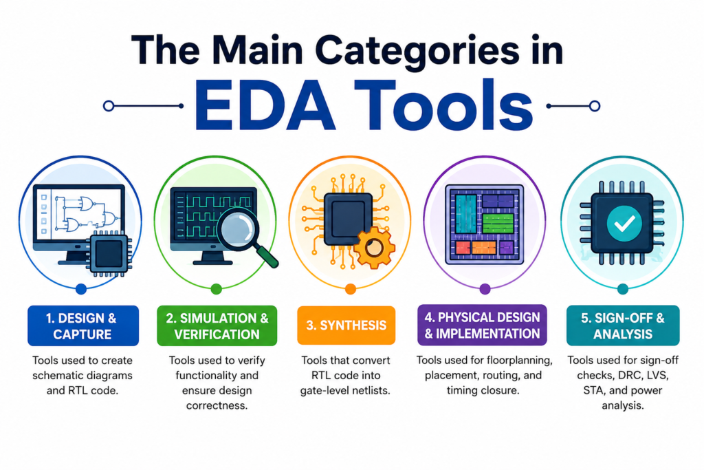
EDA isn’t a single tool — it’s an entire toolchain, and understanding the categories helps make sense of the ecosystem.
Front-end design tools handle the logical description of a chip. This includes RTL design in Verilog or VHDL, functional simulation, and logic synthesis, where a design description is converted into a gate-level representation.
Verification tools check that a design actually does what it’s supposed to do. Formal verification, simulation-based testing, and emulation platforms all fall here, and this stage often consumes more engineering time than the design itself.
Physical design and implementation tools take the verified logic and turn it into an actual layout — floorplanning, placement, clock tree synthesis, and routing all happen at this stage, shaping how the chip will physically sit on silicon.
Signoff and physical verification tools perform the final checks before tape-out, confirming timing closure, power integrity, and manufacturability rules are all met.
Analog and mixed-signal tools handle a different design style entirely, focused on custom transistor-level layout for circuits like amplifiers, converters, and RF components that can’t be automated the same way digital logic can.
Each category depends on the others, and a real chip development flow moves through all of them, often looping back multiple times as issues surface.
Synopsys, Cadence, and Siemens: The Companies Behind the Tools

Three companies effectively define the EDA industry, and together they account for the large majority of tools used at chip companies worldwide: Synopsys, Cadence Design Systems, and Siemens EDA (formerly known as Mentor Graphics).
Synopsys EDA tools are widely regarded as the industry benchmark for synthesis and signoff. Design Compiler remains one of the most deployed synthesis tools in the world, PrimeTime is a standard for timing signoff, and IC Compiler II handles physical implementation. Synopsys has also expanded well beyond traditional chip design software — its acquisition of Ansys brought multiphysics simulation capabilities directly into the EDA flow, letting engineers analyze electromagnetic, thermal, and mechanical effects earlier in the design process rather than discovering problems after tape-out.
Cadence takes a strong position in custom and analog layout with Virtuoso, and its Innovus and Genus tools are increasingly common choices for advanced-node digital implementation. Siemens EDA doesn’t offer a flagship synthesis tool but dominates physical verification through Calibre, which runs on nearly every chip that reaches manufacturing.
Knowing which company’s tools are used for which stage matters because most real design flows mix and match — a team might synthesize with one vendor’s tool and sign off with another’s, depending on what’s proven reliable at a given process node.
How AI Is Reshaping EDA Software for Chip Design

The biggest shift in EDA software for chip design over the past couple of years has been the move toward AI-assisted and increasingly autonomous workflows. Tools like Synopsys DSO.ai and Cadence Cerebrus use machine learning to explore design space automatically, testing thousands of configuration options to find layouts that hit power, performance, and area targets faster than manual iteration ever could.
This isn’t a minor efficiency gain. As chips move to smaller process nodes with gate-all-around transistors, backside power delivery, and multi-die packaging, the number of design rule checks and possible configurations has grown by an order of magnitude compared to older nodes. AI-driven exploration is becoming less of a convenience and more of a necessity just to keep design schedules realistic. Recent announcements have pushed this even further, with agentic AI workflows that can take a design from specification closer to a finished implementation with less manual intervention at each stage.
Latest Trends Shaping the EDA Industry

A few developments are worth watching if you want to understand where chip design tools are headed next.
Multi-die and chiplet-based architectures are becoming mainstream, driven by the difficulty and cost of scaling a single monolithic die at advanced nodes. EDA vendors have responded with tools specifically built for 2.5D and 3D packaging, where multiple chiplets need to be verified as if they were one system.
Foundries and EDA companies are now co-developing certified toolchains for the newest process nodes, meaning a design flow is validated end-to-end for a specific node before customers even start their projects. This tighter foundry-EDA collaboration is shortening the gap between a new process becoming available and chips actually being designed on it.
Cloud-based EDA is also expanding access to compute-heavy verification and simulation work, letting teams burst capacity for large jobs instead of relying solely on on-premises server farms. And geopolitics has entered the picture too — export controls have pushed some regions to invest heavily in developing their own domestic EDA capabilities, which is starting to reshape the competitive landscape outside the traditional three major vendors.
1. What are Synopsys, Cadence, and Siemens known for?
Synopsys, Cadence, and Siemens are leading EDA companies providing software for chip design, verification, simulation, physical design, and semiconductor development.
2. What are EDA tools in VLSI?
EDA tools are software platforms used by VLSI engineers to design, simulate, verify, analyze, and optimize integrated circuits before semiconductor manufacturing.
3. Which companies provide the best EDA tools?
Synopsys, Cadence, and Siemens EDA are major providers of professional EDA tools widely used across semiconductor and VLSI design workflows.
4. What EDA tools does Synopsys provide?
Synopsys provides tools for synthesis, simulation, verification, physical design, timing analysis, and semiconductor IP used across modern chip development.
5. What is Siemens EDA used for?
Siemens EDA provides tools for IC verification, simulation, PCB design, semiconductor testing, and electronic system development across complex chip projects