

India Offers Chip Design, Gear Subsidy From $13.4 Billion Fund

What if the biggest bottleneck in India’s semiconductor dream isn’t the chips at all, but the machines and chemicals nobody in the country knows how to make yet? That’s the uncomfortable truth behind India’s newest announcement, and it’s why this fund is getting more attention from industry watchers than almost any policy move since the chip mission first began.
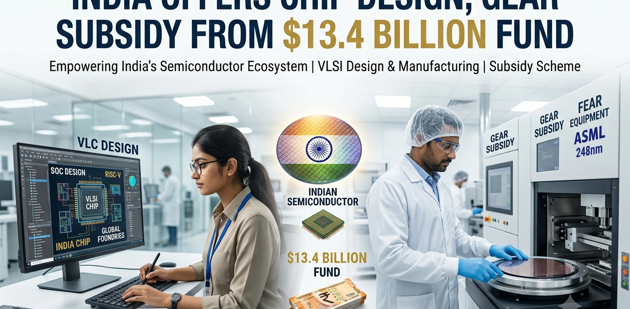
The Union Cabinet has cleared an outlay of roughly ₹1,27,500 crore, close to $13.4 billion, under a scheme widely referred to as Semicon 2.0. The money is aimed squarely at two things India has struggled with for years: designing chips domestically instead of outsourcing the intellectual work, and building the equipment, chemicals, and gases that every fab needs but almost none of which are made on Indian soil today.
What Semicon 2.0 Actually Funds
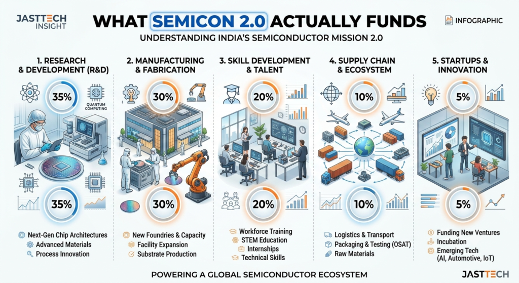
Semicon 2.0 is built around six distinct pillars, and each one targets a different weak spot in the supply chain rather than repeating what the first phase already covered. Chip design and homegrown intellectual property sit at the center, extending the earlier Design-Linked Incentive approach that already helped dozens of design startups get access to expensive electronic design automation tools. Alongside design, there’s dedicated support for additional wafer fabrication plants, with capital expenditure support reportedly running as high as 40 percent for silicon-based fabs and slightly less for compound semiconductor units built around materials like gallium nitride and silicon carbide. Assembly, testing, and packaging get their own pillar too, with a clear push toward advanced techniques like chiplet integration and 3D die stacking rather than just basic packaging work. Research, training infrastructure, and long-term workforce development round out the framework, backed by hundreds of crores earmarked specifically for research centers over the coming fiscal year.
The New Piece: Machines and Materials
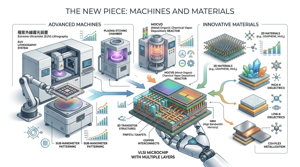
The genuinely new addition in this round is the machines-and-materials pillar, and it exists because of a problem India’s first phase exposed rather than solved. Even as packaging plants in Gujarat began shipping real, commercial chips over the past year, almost none of the equipment or chemistry running inside those plants was made domestically. Industry estimates suggest more than 90 percent of the specialized equipment and roughly 85 to 90 percent of the specialty chemicals and electronic-grade gases used in Indian fabs are still imported, largely from Japan, Germany, the United States, and the Netherlands. Semicon 2.0 responds with a flat 30 percent incentive on project cost for companies willing to manufacture that equipment and chemistry inside India, whether they’re existing Indian industrial players or global suppliers looking to localize. It’s a deliberate attempt to build the supply chain behind the fabs, not just the fabs themselves.
From Announcements to Actual Chips
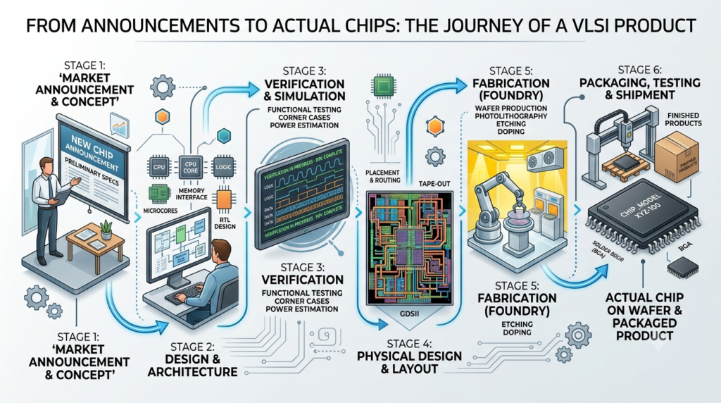
Unlike earlier chapters of India’s chip story, this fund isn’t launching into a policy vacuum. Three facilities in Sanand, Gujarat are already packaging and testing commercial chips, including a large memory assembly plant that began shipping DRAM and NAND modules earlier this year, alongside two other packaging operations that reached commercial production within the last several months. A fourth site is expected to come online before the year is out. This matters because it separates Semicon 2.0 from the earlier waves of semiconductor promises that never made it past the announcement stage, most notably a well-known 2005 attempt that collapsed after imported equipment got stuck in customs delays for months. The government has clearly learned from that failure on the process side, but the challenge this time is different: building an industrial base for precision manufacturing equipment and ultra-pure chemistry from close to zero, which is less a bureaucratic hurdle and more a decades-long engineering problem that other countries took generations to solve.
Where India’s Real Advantage Lies

None of this means India is trying to out-compete Taiwan or the United States on leading-edge chip fabrication anytime soon, and most serious analysts don’t expect that to be the near-term goal. The advantage India brings to the table is a mix of design talent, a rapidly growing domestic appetite for chips, and a geopolitical position that global manufacturers increasingly see as a useful counterweight to concentration in East Asia. Domestic chip consumption is projected to more than double over the next several years, creating a home market that can absorb production even before export demand kicks in fully. India is also home to a notably large share of the world’s chip designers, though most of that talent has historically been used for contract design work rather than for building Indian-owned intellectual property. Semicon 2.0’s design pillar is specifically structured to change that ratio, turning engineering skill that already exists into chips and IP that are actually owned in India rather than licensed out.
Whether this fund becomes the turning point that finally closes India’s equipment and materials gap, or simply another well-funded ambition that takes a decade longer than planned, will likely become clearer at the country’s major industry showcase later this year, where global equipment and chemical suppliers are expected to signal how seriously they’re taking the offer. For now, Semicon 2.0 is the clearest sign yet that India’s semiconductor strategy has moved past just attracting factories and started tackling the much harder problem of what runs inside them.