


PSG Tech Signs MoU with Krivya Semicon to Boost VLSI Testing

Semiconductor chips power almost everything we touch today, yet very few institutions in India get the chance to work directly with the companies that test these chips before they reach the market. That gap just got a little smaller. On 17 July 2026, PSG College of Technology, Coimbatore, signed a Memorandum of Understanding with Krivya Semicon, a Bengaluru-based VLSI testing company, and the move could quietly reshape how testing talent is built in the region.
The partnership is not just a symbolic handshake. It brings together an academic institution with decades of engineering credibility and a company that specializes in some of the toughest problems in chip testing today. For anyone tracking India’s growing footprint in semiconductors, this MoU is worth a closer look, because it signals where the industry expects its next wave of testing expertise to come from.
What the MoU Actually Covers

The agreement was signed in the presence of Kamlesh Pandey, Founder and CEO of Krivya Semicon, along with Manivannan Ethiraj, Senior Manager – Engineering at the company. Thyla, Principal (FAC) of PSG College of Technology, represented the institution at the event. According to details shared around the signing, the MoU is built around five core areas: joint research, consultancy, internships, industry-oriented training, and expert lectures.
This is a broader scope than many campus-industry tie-ups, which often stop at guest lectures or one-off internship slots. Here, the intent seems to be a continuous exchange, where research problems from the industry side can flow into the institution, and practical, hands-on exposure can flow the other way. That two-way structure is usually what separates a genuinely useful MoU from a paperwork exercise.
Why Krivya Semicon Matters in This Deal

Krivya Semicon isn’t a generic electronics firm dabbling in chip testing. The company works specifically on Design-for-Test architecture, a discipline that decides how easily a chip can be tested once it’s manufactured. Their focus areas include Logic BIST, scan architecture, ATPG, Memory BIST, JTAG boundary scan, and IJTAG implementation, along with alignment to IEEE testing standards.
These aren’t buzzwords picked for a press note. Each of these techniques solves a real bottleneck in semiconductor manufacturing. Test time, for instance, is one of the most expensive parts of chip production, and companies that can shrink it without sacrificing reliability have a genuine competitive edge. By bringing this kind of specialized knowledge onto a college campus, the collaboration gives PSG Tech access to problems that most academic labs rarely get to work on directly.
The Placement and Training Angle

During the visit, the Krivya Semicon team also met with Nadarajan, Dean of Placement and Training at PSG Tech, to discuss future collaboration around internships and industry engagement. This part of the visit is easy to overlook, but it may end up being just as important as the research component.
Placement conversations that happen alongside an MoU signing tend to move faster than ones that get scheduled separately later. It suggests that both sides are thinking beyond a one-time project and are instead trying to build a pipeline, one where people trained under this partnership can transition into real roles within the VLSI testing ecosystem without a long gap between learning and working.
What This Means for India’s VLSI Testing Ecosystem
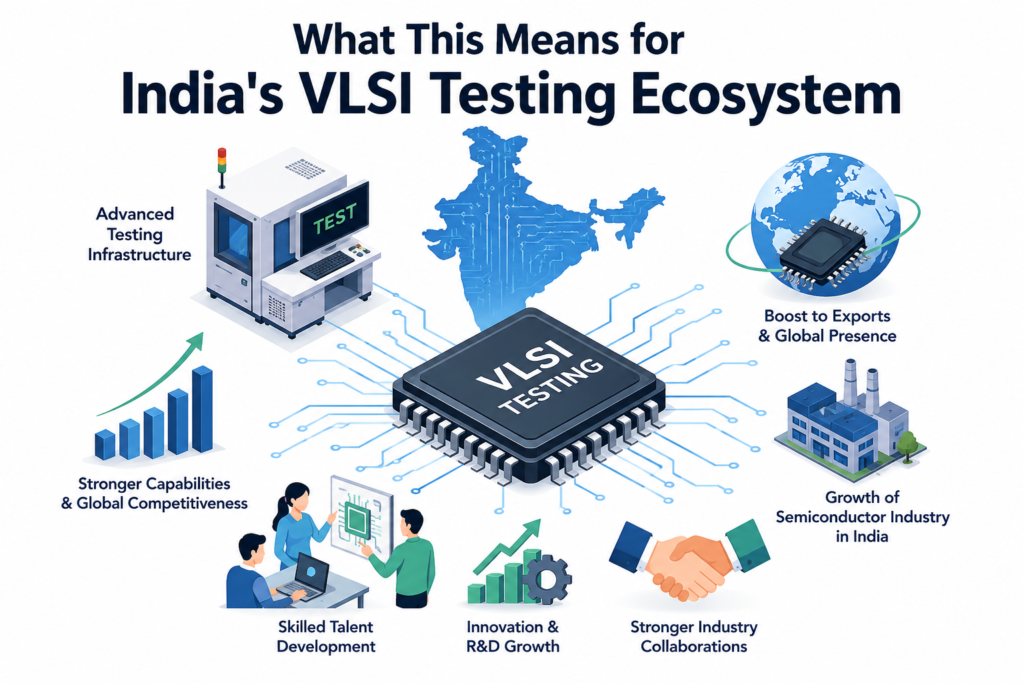
India’s semiconductor ambitions have been widely discussed over the past few years, with government missions and private investment both pushing for a stronger design and testing base within the country. But policy announcements alone don’t create skilled engineers. That happens through exactly this kind of ground-level partnership, where a company with real testing expertise sits down with an institution that has the infrastructure and the talent pool to absorb that knowledge.
Coimbatore, where PSG Tech is based, has historically been known more for its industrial and textile manufacturing than semiconductors. A partnership like this could nudge the region’s engineering ecosystem a little closer to the electronics design and testing map, alongside more established hubs like Bengaluru. It also reflects a pattern seen elsewhere in the country, where testing and design houses are increasingly choosing to build relationships with institutions outside the usual metro clusters.
For Krivya Semicon, the MoU extends its reach beyond Bengaluru and gives it a direct line into a talent base in Tamil Nadu, a state that has been steadily investing in electronics and semiconductor-linked infrastructure. For PSG Tech, it adds a specialized, industry-tested layer to its VLSI-related programs, something that textbooks and simulations alone cannot fully replicate.