


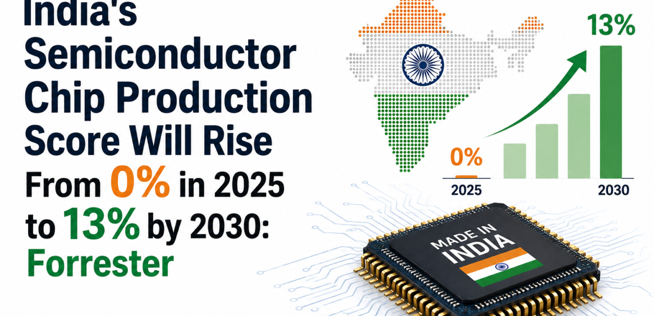
India’s Semiconductor Chip Production Score Will Rise From 0% in 2025 to 13% by 2030

Imagine a country that designs a fifth of the world’s chips but has never fabricated a single one on its own soil — that is India in 2025, and it is about to change in the most consequential industrial bet the nation has made in a generation.
For decades, India built the software, wrote the design code, and trained the engineering workforce behind the world’s semiconductors, yet every chip inside every phone, car, and data centre in the country was made somewhere else. That is now shifting. Government roadmaps point to a jump from near-zero domestic chip fabrication today to a 10-13% share of the global semiconductor value chain by 2030, backed by a chain of fabs, packaging units, and policy incentives that have moved from paperwork to construction sites in barely three years.
From Blueprint to Bedrock: Why India Starts at Zero
India’s semiconductor story until now has been almost entirely a design and import story. The country buys the overwhelming majority of the chips it uses from abroad, spending well over a hundred billion dollars on imports over the past several years. There has never been a large-scale commercial fab operating on Indian soil, which is why the starting point on any production scorecard reads close to zero.
That gap is exactly why the government treats domestic fabrication as a national priority rather than just an economic one. Heavy reliance on imported chips creates exposure during global supply disruptions, and it leaves critical sectors like defence and telecommunications dependent on foreign supply chains. The push toward a 10-13% share of global chip capacity by 2030 is less about chasing a number and more about closing a structural vulnerability that became painfully visible during the worldwide chip shortages of recent years.
Inside the Fabs: Dholera, Sanand, and the New Chip Map

Gujarat has emerged as the physical centre of this shift. The flagship project is Tata Electronics’ fabrication plant in Dholera, built in partnership with Taiwan’s Powerchip Semiconductor Manufacturing Corporation, with a planned capacity of 50,000 wafer starts a month. The facility, notified as a special economic zone earlier this year, is targeting its first silicon by late 2026, starting with the mature 28-nanometre node before eventually moving toward 22nm. That single milestone would mark the first time a semiconductor is actually fabricated inside the country rather than merely designed here.
Around that anchor project, a wider ecosystem has taken shape faster than most observers expected. Micron’s assembly and test facility in Sanand was inaugurated by the Prime Minister earlier this year and is already packaging memory chips, with output expected to scale from tens of millions of units this year to hundreds of millions next year. CG Power’s OSAT unit in Sanand, Kaynes Semicon’s packaging facility that reached commercial production just over a year after breaking ground, and Tata’s assembly and test plant in Assam round out a cluster of projects that together mark the shift from policy documents to operating machinery.
The Money and the Mission: How India Plans to Fund Its Leap

None of this comes cheap, and the funding trail tells its own story about how seriously the effort is being taken. The original semiconductor mission carried an outlay of roughly ten billion dollars in fiscal support, split between fabrication and packaging schemes. Mid-2026 brought a further commitment of over thirteen billion dollars in fresh government backing for design, production equipment, and supply-chain infrastructure, on top of the earlier funding.
The private side has matched that ambition. Tata’s Dholera investment alone runs into the tens of thousands of crores, and additional projects — including a silicon carbide compound semiconductor fab in Odisha and new discrete-semiconductor capacity in Gujarat and Surat — have been approved under the same mission. By mid-2026, more than a dozen semiconductor projects were operational or under active development across the country, a pace of expansion that would have seemed unrealistic just a few years earlier.
Talent, Technology, and the Long Road to 13%

Building a fab is only half the challenge; running one profitably for decades is the harder part. India’s roadmap acknowledges several structural barriers on the way to its 2030 target: the technical complexity of advanced fabrication, the scarcity of experienced process talent, the sheer capital intensity of the industry, and the difficulty of winning market share from entrenched suppliers in East Asia. Without access to the most advanced lithography tools used for cutting-edge nodes, India’s near-term strategy leans on mature technology and trusted-partner arrangements rather than trying to leapfrog straight to the industry’s bleeding edge.
That is also why the near-term targets are calibrated the way they are. Reaching a double-digit share of global chip capacity by 2030 does not require competing head-on with the most advanced fabs in Taiwan or South Korea. It requires steadily building out mature-node fabrication, packaging, and testing capacity across multiple sites, while developing a domestic workforce capable of running that infrastructure over the long term. The government’s own projections suggest India could be counted among the world’s top chip ecosystems by the end of this decade — not by matching the most advanced players on technology, but by capturing a meaningful, growing slice of a trillion-dollar global market.
The gap between 0% and 13% looks small on paper, but it represents the difference between a country that has never made a chip and one that has built an entire fabrication and packaging supply chain from the ground up in under a decade. Whether India hits that number on schedule will depend on execution at Dholera and the dozen projects around it — but for the first time, the infrastructure to make it possible actually exists.