




Physical Design Interview Preparation: 25 Technical Questions Explained

Breaking into the semiconductor backend domain requires far more than memorizing textbook definitions of CMOS fabrication or basic digital logic gates. Hiring managers at top fabless companies and design service firms evaluate candidates on how they handle real-world silicon trade-offs involving Power, Performance, and Area (PPA). During technical rounds, interviewers present practical scenarios—such as sudden routing congestion around macro channels, setup failures after clock tree synthesis, or dynamic voltage drops during peak switching—to test your debugging methodology. Approaching your preparation systematically across every stage of the netlist-to-GDSII flow ensures you can articulate both the theoretical physics and the EDA tool commands behind every design closure decision.
Before diving deep into tool-specific scripting and advanced node signoff checks, candidates must establish clarity on how backend implementation differs from frontend logic coding. Many engineering graduates spend months comparing physical design versus RTL design career paths before committing to the physical implementation track, where spatial geometry, parasitics, and manufacturing rules govern daily engineering work. Once you decide to pursue backend engineering, your interview readiness depends on mastering the complete physical implementation pipeline—from initial sanity checks on synthesized netlists to final DRC and LVS verification. The twenty-five questions below reflect the exact technical depth expected across campus placements and experienced lateral interviews.
Netlist-to-GDSII Flow & Input Sanity Checks
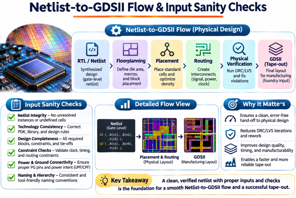
Before running placement or routing algorithms, a physical design engineer must validate input files to prevent downstream tool crashes and inaccurate timing models.
- What are the mandatory input files required to start a Physical Design flow?You need the synthesized gate-level netlist (
.v), standard cell and macro timing libraries (.lib), physical layout abstracts (.lef), Synopsys Design Constraints (.sdc), technology files (.tf), and parasitic extraction lookup tables (.tluplusor.captable). - What sanity checks do you perform before starting floorplanning? Engineers check for floating inputs, multi-driven nets, combinational loops, assign statements, missing timing arcs in
.lib, mismatches between.lefand.libcell definitions, and unconstrained timing paths in the.sdcfile. - What is the difference between Technology LEF and Cell LEF? Technology LEF contains foundry-specific metal layer rules, via definitions, spacing, and width constraints. Cell LEF defines the physical boundary, pin geometries, obstructions, and site class of individual standard cells and macros without exposing internal transistor layouts.
- Why are physical-only cells like Tap cells and End-cap cells added early in the flow? Well-tap cells connect the N-well to VDD and P-substrate to VSS at regular intervals to prevent latch-up. End-cap cells sit at row boundaries to protect standard cell gate poly from lithographic edge distortion and maintain well continuity.
Floorplanning & Power Grid Architecture
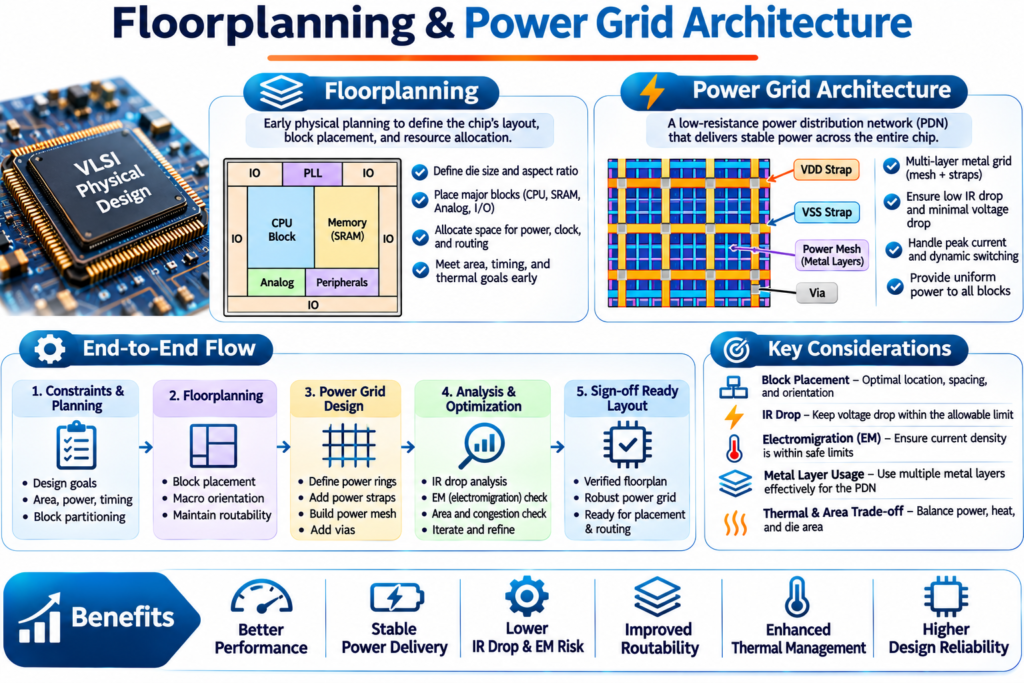
Floorplanning defines the physical foundation of the chip, where early decisions on die dimensions, macro placement, and power straps dictate whether the block can achieve timing and routing closure later. Interviewers test how candidates calculate core utilization targets, allocate routing channels between memories, and place blockages or halos to stop standard cells from crowding macro pins. You must also explain how power rings, vertical and horizontal power stripes, and decoupling capacitors work together to suppress static and dynamic IR drop across high-activity logic regions.
Building strong intuition around macro flylines and power grid resistance separates confident backend candidates from those who only memorize command sequences. While reviewing core VLSI interview questions for ECE graduates builds a solid digital electronics baseline, backend interviews specifically probe how physical distance and metal layer resistance degrade supply voltage at the transistor level. Demonstrating that you can diagnose whether a voltage drop stems from insufficient upper-layer power stripes or missing local decoupling capacitors shows real project readiness.
- How do you determine optimal macro placement during floorplanning? Place macros along the core periphery so central area remains open for standard cells. Use flyline analysis to align macro pins toward connected logic, orient pins facing the core, and maintain sufficient channel spacing for routing tracks and power stripes.
- What is the difference between a Macro Halo and a Placement Blockage? A halo is a keep-out margin attached directly to a macro that moves automatically whenever the macro is relocated. A placement blockage is a fixed coordinate region on the floorplan where standard cells are restricted either completely (hard) or partially (soft/partial).
- How do you calculate core utilization, and why avoid 95% utilization?Core utilization equals total standard cell area divided by available core placement area. Targeting 95% leaves zero whitespace for timing optimization buffers, clock tree insertion, and ECO cells, causing severe routing congestion and DRC shorts.
- How do you mitigate Static and Dynamic IR Drop during power planning? Static IR drop is reduced by widening upper metal power stripes, increasing strap density, and adding via pillars. Dynamic IR drop—caused by simultaneous switching—is mitigated by inserting decoupling capacitor (decap) cells near high-toggle logic.
Standard Cell Placement & Congestion Optimization
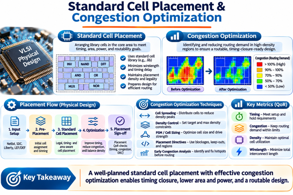
Once the floorplan and power mesh are locked, placement engines optimize standard cell coordinates for wirelength, timing, and routability.
- What causes placement congestion, and how do you resolve it?Congestion stems from high local cell density, pin-dense standard cells (like AOI/OAI gates), and narrow macro channels. Fixes include applying partial placement blockages, enabling cell padding, spreading high-pin-density cells, and adjusting macro spacing.
- What is High Fanout Net Synthesis (HFNS)? Before clock tree synthesis, non-clock signals with massive fanout—such as reset, scan enable, or set pins—suffer huge transition delays. HFNS builds balanced buffer trees to split the capacitive load and meet maximum transition limits.
- Why do we use Multi-Vt cells during placement optimization? Low-Vt (LVT) cells switch rapidly and close setup violations on critical paths, though they consume high leakage power. High-Vt (HVT) cells have higher threshold voltages, reducing static leakage on non-critical paths while increasing cell delay.
- What is the purpose of Tie-High and Tie-Low cells? Connecting gate inputs directly to VDD or VSS rails exposes delicate thin gate oxides to voltage surges and ESD damage. Tie-high and tie-low cells safely clamp constant logic inputs using transistor-based voltage division.
Clock Tree Synthesis (CTS) & Skew Management
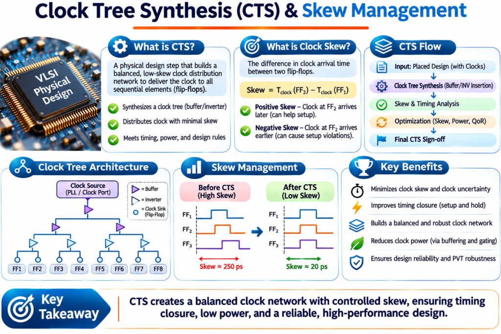
CTS builds the physical clock distribution network from the clock root pin to every sequential clock sink, transitioning the design from ideal clocks to propagated clocks.
- What are the primary goals of Clock Tree Synthesis?CTS aims to minimize clock skew across synchronous registers, control overall insertion delay (latency), maintain sharp clock transition times (slew), and minimize dynamic clock power.
- Why are clock buffers and inverters preferred over normal data cells in CTS? Clock buffers and inverters are designed with symmetric rise and fall times (50% duty cycle preservation) and balanced P/N transistor ratios, preventing pulse width degradation across long clock chains.
- What is Useful Skew, and when is it applied? Useful skew intentionally delays or advances clock arrival at specific capture or launch flip-flops to borrow timing slack from adjacent paths, helping close stubborn setup violations without resizing data path gates.
- Why do we apply Non-Default Rules (NDR) on clock nets? Clock nets toggle every cycle and drive heavy loads. Applying NDRs—such as double width and double spacing—lowers wire resistance to improve slew and increases spacing to shield clocks from crosstalk noise.
Routing, Signal Integrity & Crosstalk
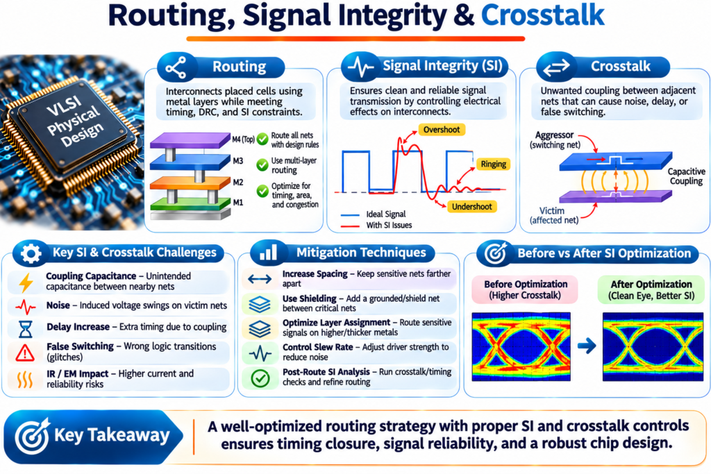
Routing converts logical net connectivity into physical metal geometries and vias across available metal layers while honoring foundry design rules.
- What is the difference between Global Routing and Detailed Routing? Global routing partitions the chip into coarse rectangular bins (G-cells) to plan routing topologies and estimate track congestion. Detailed routing assigns exact metal tracks, widths, and vias within each bin while resolving DRC violations.
- How does Crosstalk occur, and how do you fix Crosstalk Delay and Glitch? Crosstalk happens when capacitive coupling between adjacent parallel nets allows a switching aggressor net to distort a victim net. Fixes include increasing wire spacing, shielding sensitive nets with VSS wires, upsizing victim drivers, and inserting buffers.
- What is an Antenna Violation, and how is it resolved during routing? During plasma etching, long floating metal segments connected to a transistor gate accumulate electrical charge that can rupture the thin gate oxide. Engineers fix this by “layer jumping” to an upper metal layer near the gate or attaching a reverse-biased antenna diode.
- What are Filler cells, and when are they inserted? Filler cells are non-functional physical cells inserted into empty spaces after routing to ensure continuous N-well and implant layers across standard cell rows, satisfying foundry base-layer density rules.
Static Timing Analysis (STA), Power & Physical Signoff
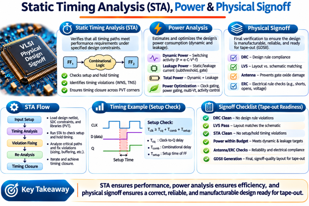
Signoff verification confirms that the routed layout meets all timing corners, electrical limits, and foundry manufacturing rules before GDSII tapeout.
- How do Setup and Hold checks differ with respect to clock frequency and PVT corners?Setup checks depend on the clock period and are typically worst at slow process, low voltage, and high temperature (SS/max corner). Hold checks are frequency-independent (checked on the same clock edge) and are usually worst at fast process, high voltage, and low temperature (FF/min corner).
- What is On-Chip Variation (OCV), and how do AOCV and POCV improve upon it? OCV applies fixed global timing derates to account for local silicon manufacturing variations. Advanced OCV (AOCV) scales derates based on logic depth and physical distance, while Parametric OCV (POCV) models cell delay statistically using mean and sigma values for less pessimistic signoff.
- What is Electromigration (EM), and how do you fix signal and power EM?Electromigration is the gradual displacement of metal atoms caused by high electron current density, leading to open circuits or shorts. Signal EM is fixed by widening wires, reducing driver strength, or splitting loads; power EM requires wider stripes and redundant via arrays.
- What are Recovery and Removal timing checks? Recovery and removal are timing checks for asynchronous control signals like asynchronous reset. Recovery specifies the minimum time the reset must be de-asserted before the active clock edge (analogous to setup), while removal specifies how long it must remain stable after the clock edge (analogous to hold).
- What is the difference between DRC, LVS, and ERC in Physical Verification? Design Rule Check (DRC) verifies that polygon widths, spacings, and densities obey foundry manufacturing rules. Layout Versus Schematic (LVS) confirms that extracted layout devices and connectivity match the golden netlist. Electrical Rule Check (ERC) flags electrical hazards like floating wells, shorted power nets, or missing well taps.
Conclusion
Preparing for a Physical Design interview is ultimately about connecting circuit theory with physical layout realities. Rather than treating floorplanning, clock tree synthesis, routing, and static timing analysis as isolated checklists, focus on how a decision in one stage cascades into timing, power, or congestion challenges downstream. By mastering these twenty-five core concepts, practicing whiteboard timing equations, and explaining trade-offs clearly, you will stand out as an engineer ready to take real silicon blocks to clean tapeout
Which EDA tools should I mention on my resume for Physical Design interviews?
Hiring managers look for hands-on familiarity with industry-standard P&R suites such as Synopsys IC Compiler II (ICC2) or Cadence Innovus, alongside signoff tools like PrimeTime (STA), StarRC (parasitic extraction), RedHawk (IR/EM), and Calibre (DRC/LVS).
How much TCL scripting knowledge is required for a fresher PD interview?
You do not need to build complex software applications, but you must write clean TCL scripts to query timing paths, filter cells or nets by attributes, automate report parsing, and execute tool-specific ECO commands.
Why do interviewers ask so many questions about Setup and Hold time?
Setup and hold equations govern every synchronous digital circuit. Interviewers use setup and hold scenarios to test whether you understand how clock skew, cell delay, wire RC parasitics, and PVT corners interact in real silicon.
What is an ECO in Physical Design, and why is it important?
An Engineering Change Order (ECO) applies targeted late-stage functional or timing fixes—such as gate resizing, buffer insertion, or spare cell rewiring—without restarting the entire placement and routing flow.
Can an Electronics and Communication Engineering (ECE) graduate get into Physical Design without an M.Tech?
Yes. While an M.Tech in VLSI helps, B.Tech/B.E. graduates who build strong fundamentals in CMOS circuits, Static Timing Analysis, Unix/TCL scripting, and complete at least one RTL-to-GDSII block project routinely clear campus and off-campus interviews.
How does technology node scaling (e.g., 7nm or 5nm) change PD interview questions?
At advanced FinFET nodes, interviews emphasize multi-patterning coloring rules, via resistance dominance over wire resistance, POCV statistical timing, local layout effects (LLE), and strict electromigration limits.
What is the single biggest mistake candidates make during PD technical rounds?
Many candidates memorize textbook definitions without understanding cause-and-effect trade-offs—for example, suggesting upsizing a cell to fix setup without recognizing that it increases input capacitance and can degrade the previous stage’s transition time.