

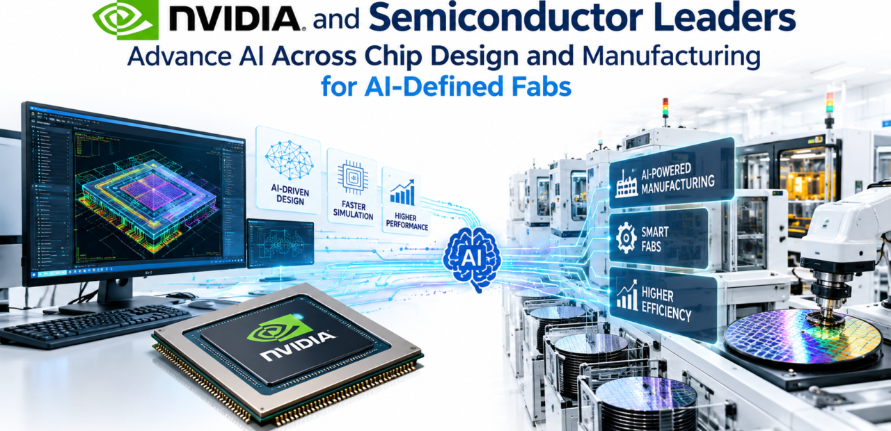
NVIDIA and Semiconductor Leaders Advance AI Across Chip Design and Manufacturing for AI-Defined Fabs

The semiconductor industry is embracing AI-defined fabs to meet growing demand for smaller, faster, and more power-efficient chips. NVIDIA and industry leaders are integrating GPU-accelerated computing, AI agents, and physics-based simulations into semiconductor design and manufacturing to improve efficiency, quality, and yield.
With advanced CUDA-X libraries and AI-powered tools, companies such as Synopsys, Cadence, Lam Research, KLA, and Applied Materials are transforming VLSI workflows. By combining AI with digital twins and automated inspection, these technologies enable faster simulations, smarter process optimization, and more efficient chip manufacturing.
The Emergence of AI-Defined Fabs in Modern Semiconductor Manufacturing
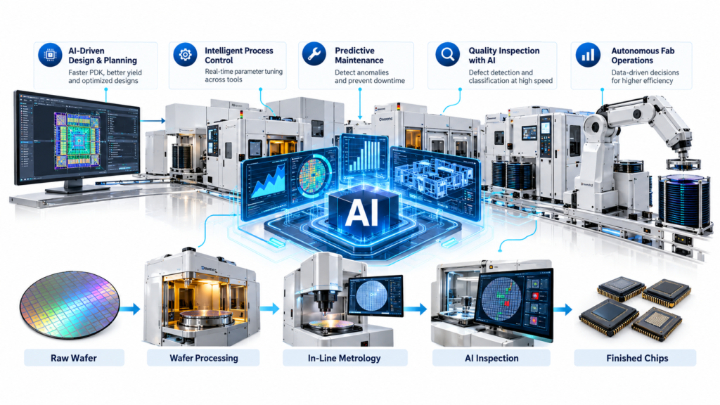
An AI-defined fab represents a modernized chip manufacturing facility where artificial intelligence coordinates process optimization, yield prediction, and complex problem resolution. As chip architectures shrink down to advanced sub-nanometer nodes, traditional manufacturing algorithms struggle to model quantum-level variations and complex physical phenomena. AI-defined fabs overcome these limits by deploying specialized software tools that continuously process sensor inputs, defect logs, and physical simulation data in real time.
By uniting physical hardware with digital twin technology, engineers can test and analyze critical process modifications inside virtual simulations before applying changes to live production lines. This capability drastically minimizes costly cleanroom trial-and-error cycles while accelerating time-to-market for cutting-edge silicon architectures.
Accelerating Atomic-Scale Simulation with NVIDIA cuPotential
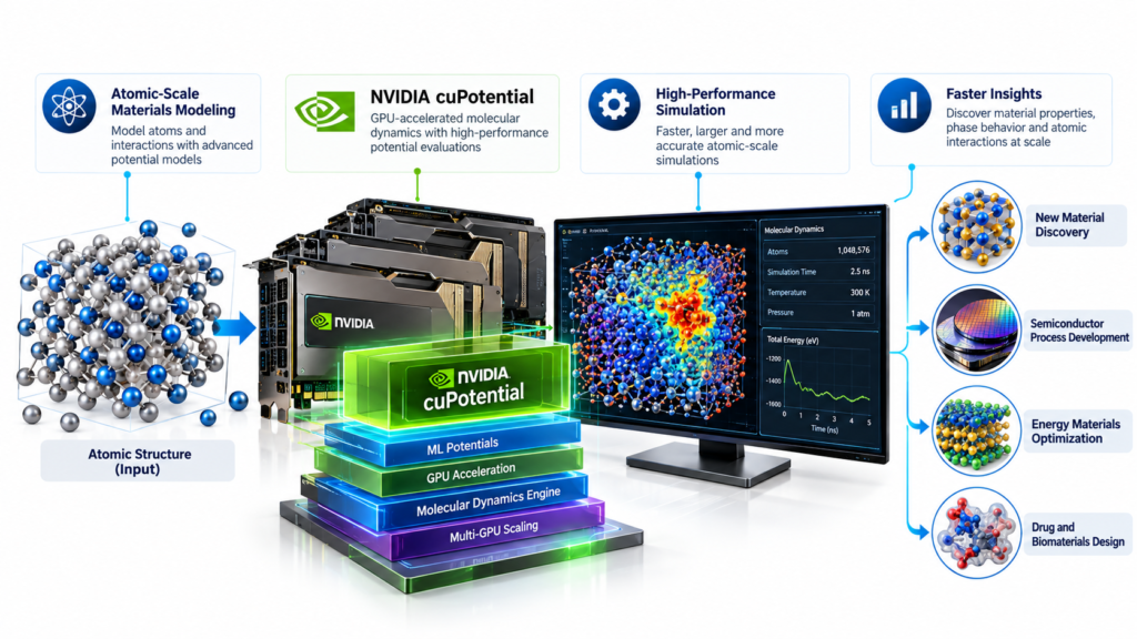
Modeling atomic and molecular interactions is fundamental to developing new semiconductor substrate materials and chemical vapor deposition processes. However, calculating quantum mechanical behavior across thousands of atoms has historically required days of intensive high-performance computing effort. NVIDIA cuPotential addresses this barrier by providing specialized, GPU-accelerated functions that integrate directly into electronic design automation software.
In early testing, cuPotential accelerated molecular dynamics and atomic calculations by an additional 2x to 3x over previously GPU-optimized baselines. When coupled with autonomous AI agents, the library enables systems to automatically test chemical configurations, evaluate atomic forces, and refine material behavior without needing continuous human intervention.
Transforming Inspection and 3D Spatial Data in Fabrication
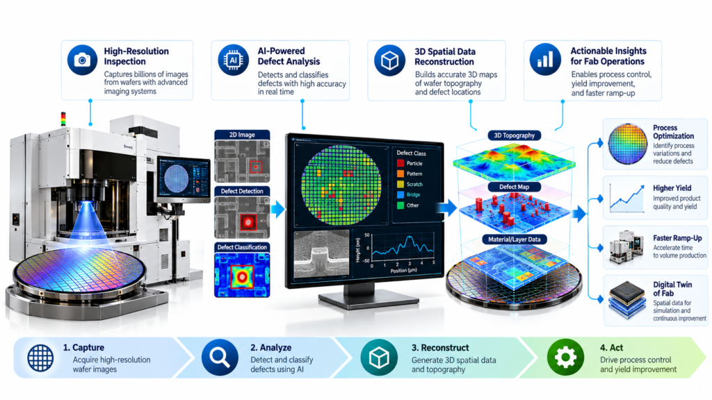
Ensuring high production yield requires wafer inspection tools that can identify microscopic manufacturing defects across trillions of microscopic features. NVIDIA NPP (Performance Primitives) and NanoVDB open-source libraries are redefining how inspection systems process ultra-high-resolution images and complex spatial datasets. Industry equipment leaders like KLA utilize GPU image processing to accelerate wafer defect analysis.
Simultaneously, Lam Research has used 3D spatial acceleration tools to speed up etch and deposition profile modeling by up to 30x. Fast 3D data modeling enables engineers to predict how physical materials build up inside microscopic trenches, preventing open circuits and electrical shorts early in the production cycle.
Industry Collaboration: EDA Partners and Equipment Leaders
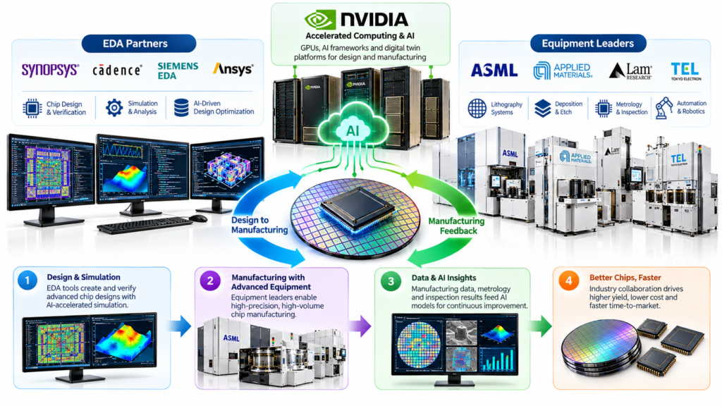
The evolution toward AI-defined fabs depends heavily on deep integration across the broader VLSI ecosystem. Design automation leaders like Synopsys and Cadence are embedding NVIDIA CUDA-X libraries directly into their modeling applications. For instance, Cadence utilizes GPU-accelerated solvers alongside specialized AI agents to optimize 3D-IC packaging designs for heat dissipation and mechanical stress up to 8x faster.
Equipment manufacturers such as Applied Materials, KLA, and Lam Research are integrating these computing technologies into physical machinery on fab floors. This software-hardware integration establishes a closed feedback loop between early physical chip layout and actual factory execution, significantly lowering design iteration costs.
Yield Optimization, Scalability, and the Future of VLSI Design
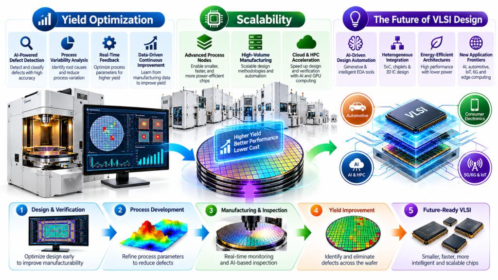
As silicon designs become increasingly intricate through chiplets and 3D stacked dies, maintaining high functional chip yields remains a primary financial priority. AI-driven digital twins and agentic simulation frameworks allow engineering teams to detect structural anomalies, thermal bottlenecks, and manufacturing variances long before mass production begins.
Looking ahead, automated engineering platforms powered by AI agents promise to streamline end-to-end chip development—from initial functional specifications down to graphic data system files. The widespread adoption of accelerated computing across fabs helps the industry keep pace with rising global demands for powerful computing infrastructure while stabilizing chip fabrication costs.