

C-VISTA Can Develop Semiconductor, VLSI Solutions for Societal Applications

What if the next big chip innovation didn’t come from a corporate lab, but from a campus trying to solve a real-world problem in its own backyard? That’s exactly the idea behind C-VISTA, a new initiative that’s quietly reshaping how India thinks about semiconductor and VLSI innovation.
Held on August 3 and 4, the Founding Conclave of the Centre of Excellence for VLSI Innovation for Systems, Technology & Applications (C-VISTA) brought together voices from industry, academia, alumni networks, and government to lay the groundwork for a center focused on VLSI innovation, talent development, and industry collaboration in Coastal Karnataka. The event wasn’t just a ceremonial launch — it set the tone for how semiconductor design in India could evolve from being purely academic to being deeply rooted in solving everyday problems.
What Is C-VISTA and Why It Matters

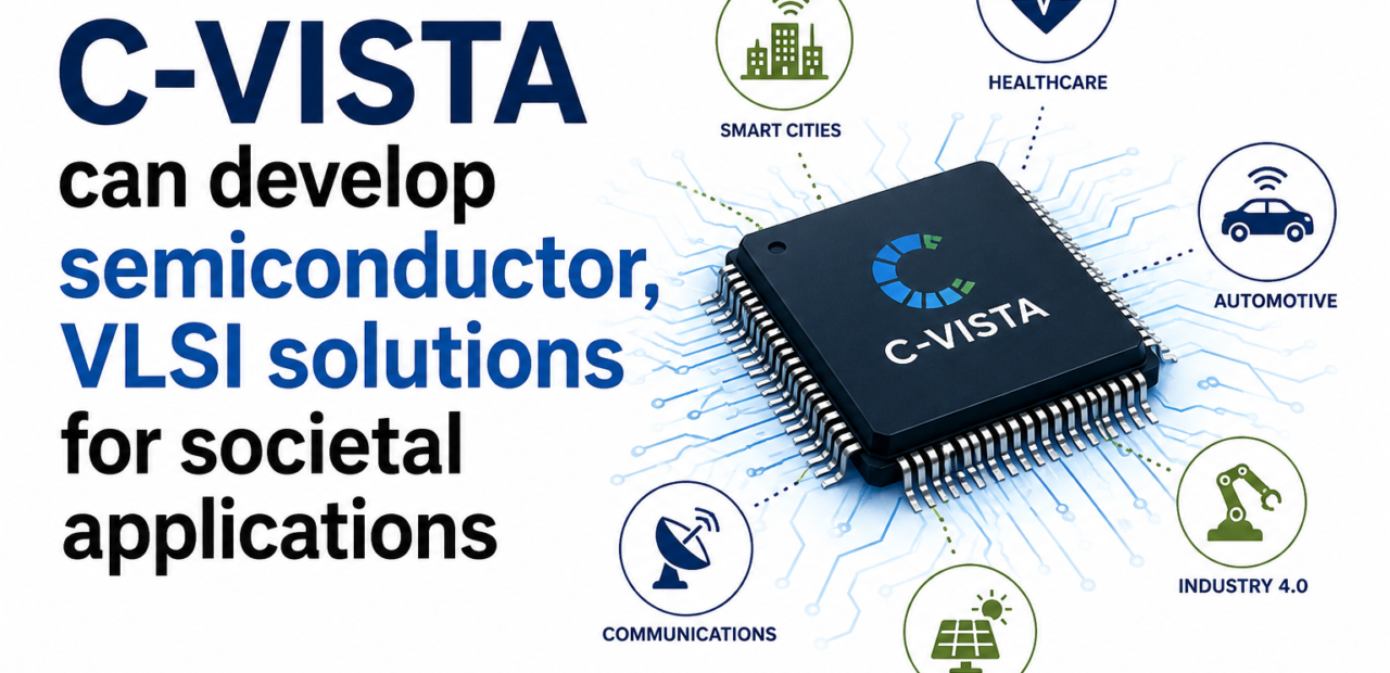
C-VISTA is being set up as a platform where research, industry expertise, and local problem-solving intersect. The idea is simple but powerful: instead of designing chips in isolation, the center wants to identify real, campus-level and community-level challenges and turn them into practical semiconductor and VLSI-based solutions that carry a wider societal impact. This shift matters because it moves VLSI design away from being a purely theoretical or academic pursuit and positions it as a tool for tackling tangible problems — from healthcare access to environmental resilience.
The conclave saw participation from prominent names in the semiconductor and technology space, along with organizations spanning chip design, mobility, and innovation ecosystems. A masterclass on the semiconductor value chain highlighted where India currently stands in the global chip design landscape and where the opportunities lie for the country to build stronger design and systems-innovation capabilities. This kind of open dialogue between industry veterans and academic institutions is exactly what’s needed to close the gap between what gets taught and what the semiconductor industry actually needs.
Three Founding Verticals Driving Innovation
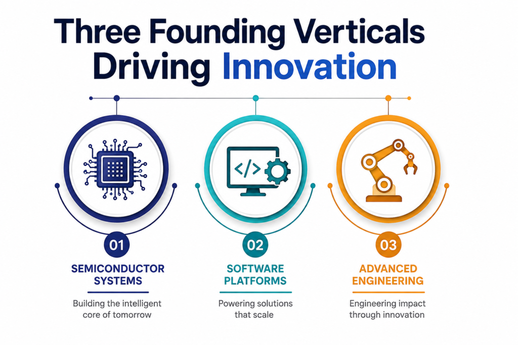
C-VISTA isn’t trying to be everything at once. Instead, it has identified three founding verticals that will guide its research and innovation efforts. The first is biomedical devices and healthcare, where VLSI-based solutions could power affordable diagnostic tools, wearable health monitors, and medical imaging systems that are urgently needed in underserved regions. The second vertical focuses on climate and disaster resilience, an area where low-power sensor networks, environmental monitoring chips, and early-warning systems built on VLSI architecture could make a measurable difference in how communities respond to extreme weather events.
The third vertical covers drones, electric vehicles, and robotics — sectors that are already booming in India and depend heavily on efficient, compact, and power-optimized chip design. By anchoring its work around these three areas, C-VISTA is signaling that the future of semiconductor design isn’t just about faster processors or smaller transistors, but about building systems that directly improve everyday life. This kind of vertical-focused approach also makes it easier for industry partners to invest in specific outcomes rather than vague research goals.
Bridging Industry and Academia for Real Impact

One of the more interesting aspects of C-VISTA is its emphasis on bridging education, research, industry partnerships, and deep-tech entrepreneurship under one roof. Panel discussions during the conclave brought together experts to examine how the center’s founding verticals could translate into workable projects, with practitioners sharing insights from their own experience in chip design, systems engineering, and product development.
This kind of collaboration model is becoming increasingly important across India’s semiconductor ecosystem. As global companies look to diversify their chip design and manufacturing footprint, institutions that can demonstrate strong industry ties and a pipeline of skilled design talent stand to benefit the most. Centers like C-VISTA could become a template for how other regions and institutions build their own semiconductor innovation hubs — ones that are less about isolated research papers and more about deployable, real-world solutions that attract long-term industry investment.
What This Means for India’s Growing VLSI Talent Pipeline
Initiatives like C-VISTA point to a larger trend in India’s semiconductor story: the growing demand for professionals trained in chip design, physical design, verification, and embedded systems. As more centers of excellence emerge across the country, the need for structured, industry-relevant training is only going to increase. This is where dedicated training hubs come into the picture. For instance, aspiring VLSI professionals in North India increasingly look toward a VLSI course in Noida to build hands-on expertise in areas like RTL design, Verilog, physical design, and verification methodologies — skills that align closely with the kind of practical, application-driven projects C-VISTA is aiming to promote.
The connection here isn’t a coincidence. As centers like C-VISTA push semiconductor innovation toward real societal applications, the demand for well-trained design engineers who understand both the theory and the practical deployment of VLSI systems will only grow. Training ecosystems that focus on current industry tools and methodologies will play a key role in feeding this pipeline, ensuring that India’s semiconductor ambitions aren’t limited by a shortage of skilled talent.