


Paras Defence Announces ₹6,200 Crore Semiconductor Plant in Madhya Pradesh

A defence company known for making optics and sensors just placed a massive bet on silicon. Paras Defence and Space Technologies has confirmed plans for a ₹6,200 crore chip packaging facility in Madhya Pradesh, and the announcement is already sending ripples through India’s semiconductor ecosystem.
The company’s wholly-owned subsidiary, Paras Semiconductors, has signed a Memorandum of Understanding with the Madhya Pradesh State Electronics Development Corporation to build an Outsourced Semiconductor Assembly and Test (OSAT) facility. This isn’t a small pilot project. It’s a full-scale greenfield plant that could reshape how India handles chip packaging, a step that comes right after the finished silicon leaves the foundry.
Coming at a time when India is racing to build a homegrown semiconductor supply chain, this move places a private defence player squarely in the middle of the country’s chip ambitions. Here’s a closer look at what’s happening, why it matters, and what it could mean for the broader industry going forward.
The Deal: What Exactly Is Being Built
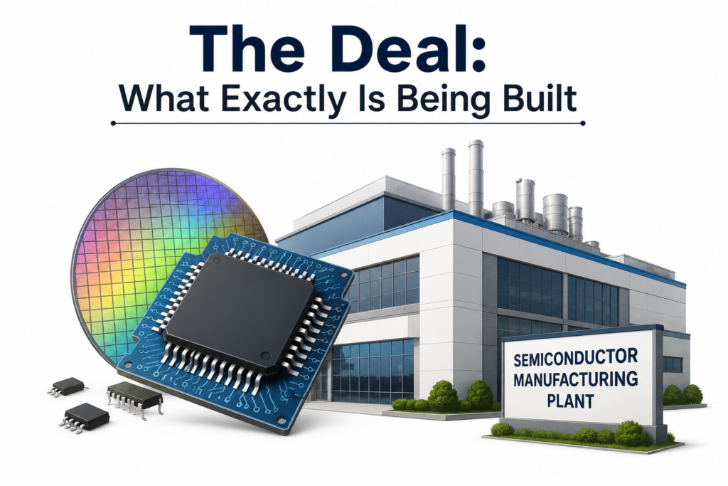
The proposed facility will come up on a 50-acre site along the Indore-Ujjain corridor in Madhya Pradesh, a stretch of land the state government has earmarked specifically for this project. The investment figure of ₹6,200 crore, roughly $644 million, positions this as one of the larger private semiconductor packaging investments announced in India this year.
Rather than manufacturing raw silicon wafers, the plant will focus on advanced chip packaging. According to details shared around the announcement, operations at the facility will include 3D heterogeneous integration, 2.5D and 3D advanced packaging, hybrid bonding, ultra-high-density fan-out packaging, chiplet integration, wafer bumping, and flip-chip assembly, along with testing and reliability checks. In simple terms, this facility will take chips that have already been fabricated elsewhere and turn them into finished, usable components ready for deployment in electronic systems.
Madhya Pradesh Chief Minister Mohan Yadav met with company officials as the MoU was exchanged, and the state government has reportedly assured full support to help the project move from paper to production without unnecessary delays.
Why OSAT Matters More Than Most People Realize

Semiconductor manufacturing is often talked about as if it begins and ends with fabrication, the process of etching circuits onto silicon wafers. But that’s only part of the picture. Once a wafer comes out of a fab, it still needs to be cut, packaged, tested, and verified before it can go into a phone, a satellite, or a missile guidance system. This is where OSAT facilities come in.
India currently imports the bulk of its packaging and testing capacity, which adds cost and time to every finished chip. A facility of this scale changes that equation for a segment of the supply chain. Advanced packaging techniques like chiplet integration are also becoming increasingly important as chip designs move away from single monolithic dies toward multiple smaller dies bonded together, a trend that’s reshaping how processors are built across the industry.
By entering this space early, Paras Semiconductors is positioning itself in a part of the value chain that’s expected to see rising demand as more fabrication units come online in India over the next few years.
What This Means for India’s Semiconductor Push
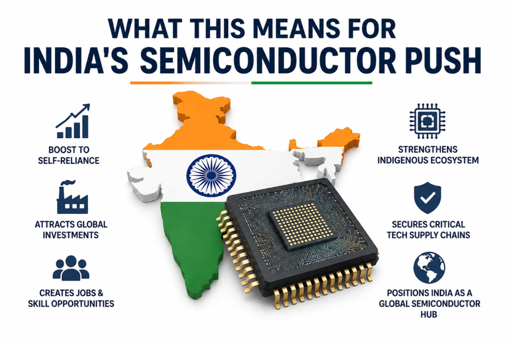
India’s semiconductor story has largely been driven by government incentives and a handful of large-scale fabrication announcements. What makes this development different is the entry of a defence-focused engineering company into the space, bringing its own balance sheet and strategic priorities into the mix.
Paras Defence has built its reputation around optics, optronics, and high-precision components for defence and space applications. Its move into semiconductor packaging isn’t a random diversification. Chips are becoming central to modern defence systems, from guidance electronics to communication modules, and having in-house or domestic access to packaged, tested chips reduces dependency on external suppliers for sensitive applications.
For Madhya Pradesh, this project adds another data point to its growing profile as a destination for high-tech manufacturing. The state has been actively courting industrial investment, and a semiconductor facility of this size gives it a foothold in a sector that most Indian states are still trying to attract.
There’s also a financial angle worth noting. Shares of Paras Defence saw mixed reactions after the announcement, with some reports noting a dip in early trade before a later recovery, a reminder that markets often take time to digest large capital commitments even when the long-term direction looks promising.
Looking Ahead: Scale, Jobs, and Future Expansion

Beyond the immediate packaging operations, there are indications the facility could eventually expand into areas like AI chip support as market demand evolves. This kind of flexibility matters in a fast-moving industry where today’s packaging technology can quickly become outdated if a facility isn’t built with future upgrades in mind.
Reports around the project also point to significant employment generation tied to this investment, with the facility expected to create thousands of jobs once operational, spanning technical, engineering, and operational roles.
For now, the project remains at the MoU stage, meaning construction timelines, hiring plans, and production targets are still likely to be firmed up in the coming months. But the intent is clear: Paras Defence wants a real presence in India’s semiconductor supply chain, not just a symbolic one.