
UPF in VLSI: Power Domains, Isolation Cells, Level Shifters and Power States Explained

As semiconductor chips scale down to advanced process nodes, managing power consumption has become as crucial as performance and area (PPA). The Unified Power Format (UPF), standardized as IEEE 1801, provides a consistent mechanism to specify power intent throughout the integrated circuit design cycle. UPF allows engineers to describe low-power strategies—such as power gating, multi-voltage domains, and retention mechanisms—independently of the underlying RTL code. By abstracting power architecture into a dedicated command set, UPF ensures that low-power intent is consistently interpreted during synthesis, physical implementation, and dynamic functional validation.
In modern low-power System-on-Chip (SoC) design, early static and dynamic verification of power intent is essential to prevent costly re-spins. Engineers utilize industry-standard VLSI simulation tools to verify UPF semantics, perform low-power checks, and detect structural issues like missing level shifters or un-isolated signals. Integrating UPF early into the design cycle guarantees that power-aware simulation models reflect real-world silicon behavior, ensuring functional correctness before tape-out.
Overview Comparison Table
| UPF Feature / Technique | Primary Purpose | Placement / Boundary | Impact on Circuit Integrity |
| Power Domains | Group logic sharing identical power/voltage specs | Module / Hierarchy level | Enables selective power-down and voltage scaling |
| Isolation Cells | Clamp floating outputs from shut-off domains | Shut-off domain outputs | Prevents X-propagation and illegal cross-conduction |
| Level Shifters | Translate signal voltage levels across domains | Voltage domain boundaries | Ensures correct logic switching and guards against breakdown |
| Power States | Define active, sleep, and transition modes | Global / System level | Orchestrates power switch sequencing and valid states |
| Retention Registers | Preserve register state during power gating | Internal to gated domains | Enables fast power-up recovery without external reload |
Understanding Power Domains in UPF
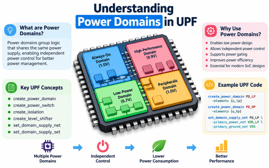
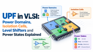
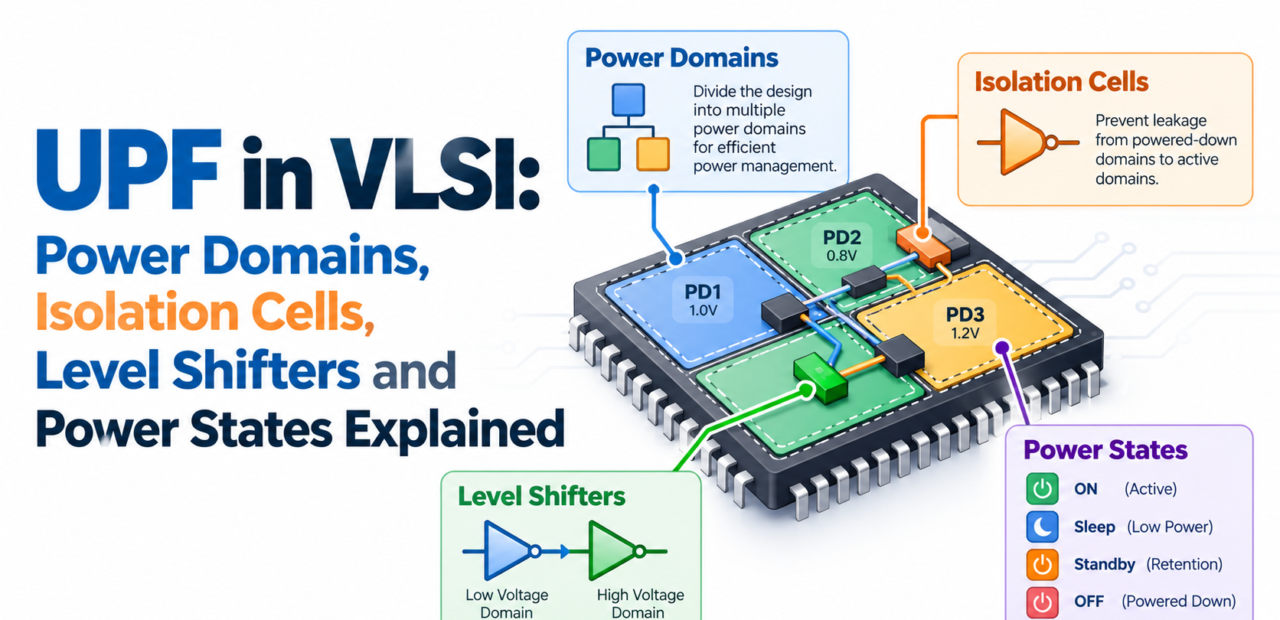
A power domain in UPF is a collection of design elements (such as logic gates, modules, or memory blocks) that share a common set of power supply requirements and operational states. Defining distinct power domains allows engineers to selectively turn off inactive portions of the chip or operate specific logic clusters at reduced voltage levels to minimize dynamic and static leakage power.
Power domains are established using the create_power_domain command in UPF. Each domain is associated with a primary supply set, defining the default power and ground connections. By dividing a monolithic design into independent power domains, designers can execute aggressive power management strategies without impacting the functional integrity of continuously active blocks.
Isolation Cells: Preventing Floating Signals
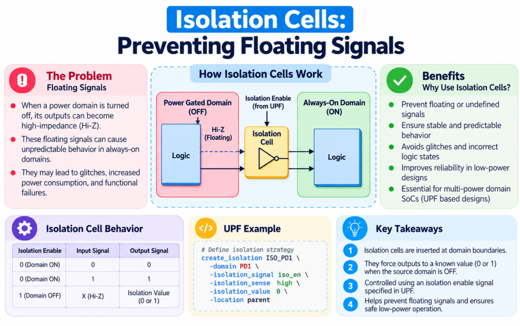
When a power domain is switched off while adjacent domains remain operational, the outputs of the powered-down domain become floating or high-impedance. These unknown signals (X-states) can propagate into powered domains, driving downstream CMOS logic into active cross-conduction states, leading to excessive current draw or functional failure.
Isolation cells are specialized logic elements inserted at the boundaries of power domains to clamp floating inputs to a deterministic logic state (logic ‘0’ or logic ‘1’). Mastery of low-power isolation concepts is a critical skill for design verification engineers, making it one of the essential VLSI interview topics evaluated during technical assessments.
Level Shifters: Bridging Multi-Voltage Boundaries
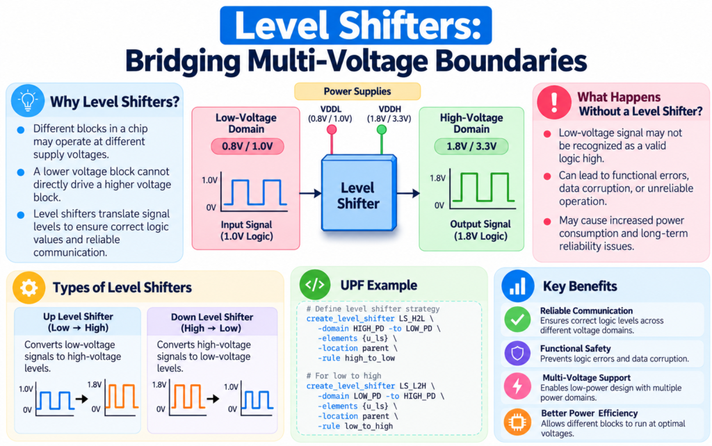
To optimize performance and power efficiency, modern ICs frequently employ multi-voltage design techniques where different logic blocks operate at varying supply voltage levels. However, driving a high-voltage logic gate directly with a low-voltage signal can cause incomplete switching, signal degradation, and increased static leakage.
Level shifters are inserted at the signals crossing different voltage domain boundaries to safely convert signal voltage amplitudes. High-to-low level shifters step down signal swings to prevent oxide overstress, while low-to-high level shifters amplify signal swings to ensure full gate turn-on at the destination domain.
Power States and State Transition Management
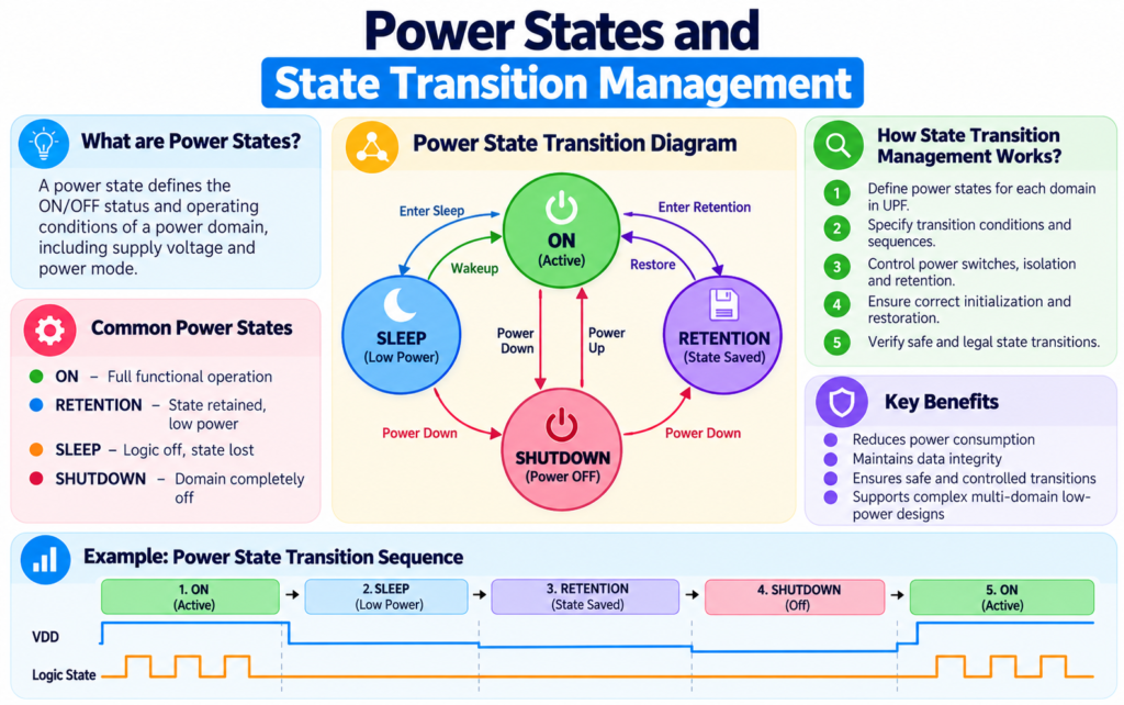
Power states define the permissible operational modes of supply sets and power domains across the chip lifecycle. An SoC typically transitions through multiple power modes—such as Full Power, Sleep, Deep Sleep, and Standby—to continuously adapt to workload requirements and minimize unnecessary power dissipation.
In UPF, power states are formally specified using add_power_state or create_pst (Power State Table) commands. Defining power states allows verification tools to validate whether illegal power state transitions occur and verify that control signals (such as isolation enable and power switch enable) follow valid temporal sequences during mode switching.
Power Gating and Retention Registers
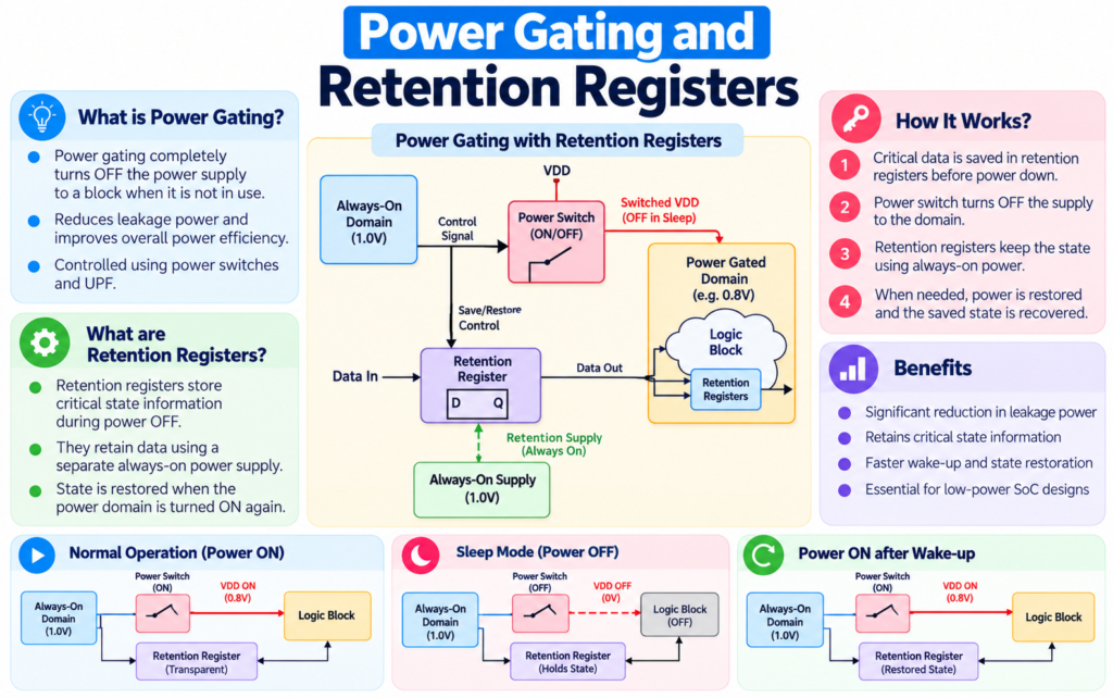
Power gating is a low-power design technique that disconnects the power or ground rail from a power domain using internal or external sleep transistors (power switches). By cutting off the supply voltage completely during idle periods, power gating effectively eliminates static leakage current—the dominant contributor to power loss in advanced sub-nanometer nodes.
Because powering down a domain flushes all internal volatile register data, retention registers are utilized to preserve critical state information. Retention registers contain a secondary shadow latch connected to an always-on power supply, enabling rapid restoring of saved state values immediately upon domain wake-up.
Conclusion
The Unified Power Format (UPF) is an indispensable standard in modern VLSI design, providing a unified methodology for specifying and verifying low-power intent across complex, multi-voltage SoCs. By systematically defining power domains, inserting isolation cells and level shifters, and declaring precise power states, hardware engineers can aggressive control static leakage and dynamic power without compromising functional reliability. As chip architectures push toward increasingly fine-grained power management, mastering UPF concepts and power-aware verification strategies remains a vital competence for modern VLSI professionals.
What is UPF in VLSI design?
UPF (Unified Power Format) is an IEEE standard (IEEE 1801) used to describe low-power intent for digital integrated circuits. It specifies power domains, power switches, isolation, and level shifting independently of RTL logic.
Why are isolation cells necessary in multi-domain power architectures?
When a power domain shuts down, its output signals float. Isolation cells clamp these signals to a known safe logic value (0 or 1) so they do not cause floating inputs, short circuits, or functional corruption in adjacent powered-on domains.
What is the difference between a high-to-low and low-to-high level shifter?
A low-to-high level shifter amplifies a low-voltage signal so it can cleanly drive higher-voltage logic. A high-to-low level shifter scales down a higher-voltage signal to prevent overvoltage stress and reliability issues in lower-voltage logic.
How does UPF differ from RTL power coding?
RTL describes functional hardware behavior, whereas UPF specifies power intent (supplies, power switches, isolation rules, and voltage domains). Keeping power specifications in UPF prevents cluttering RTL code and makes power architecture portable across synthesis and implementation stages.
What is a Power State Table (PST) in UPF?
A Power State Table (PST) defines valid combinations of voltage levels across all power domains in a chip. It helps verification tools check that the design never enters an illegal or unsupported power state during dynamic operation.
What role do retention registers play in power gating?
Retention registers store critical state data into a secondary “shadow” latch powered by an always-on supply before a domain is powered down. This allows the domain to restore its previous state quickly when power is restored.
How are UPF files validated during VLSI verification?
Verification tools parse the UPF file alongside the RTL or netlist to perform Static Power Verification (checking for missing isolation cells or level shifters) and Dynamic Power-Aware Simulation (simulating power-up/down sequences, floating values, and control signal timing).