


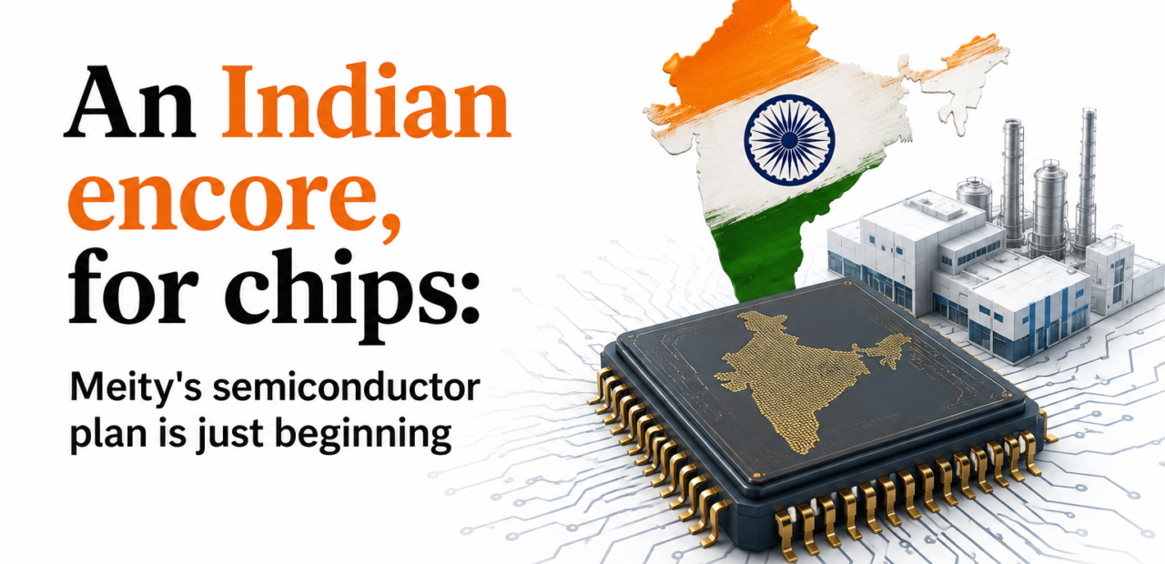
An Indian Encore, for Chips: Meity’s Semiconductor Plan Is Just Beginning

For decades, India wrote the software running the world’s chips but imported almost every chip it ever used. That long-standing equation is finally starting to flip, quietly, inside real factories rather than slide decks — and the Ministry of Electronics and Information Technology wants the shift to go a lot further, a lot faster, over the next few years.
With the Union Cabinet clearing Semicon 2.0 and backing it with a fresh outlay of roughly ₹1.27 lakh crore, chip ambitions have moved past the announcement stage. Assembly units in Sanand are already shipping packaged chips, more facilities switch on this year, and officials call 2026 a landmark moment. But the harder work — equipment, materials, design, a real supply chain — is only just beginning.
What Semicon 2.0 Actually Changes
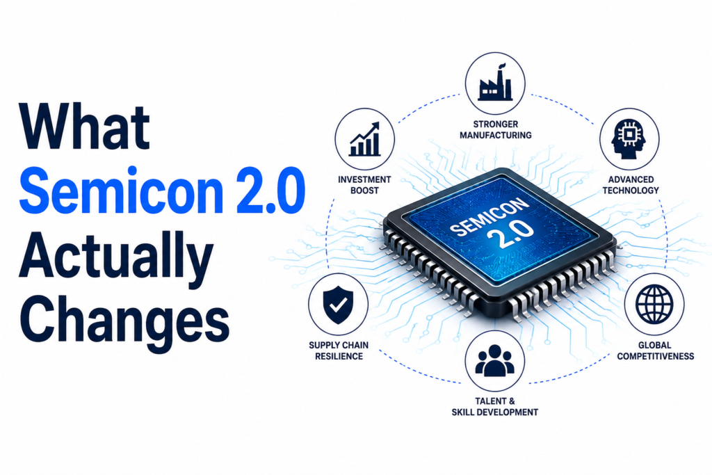
The first phase of the India Semiconductor Mission proved a point: global chipmakers were willing to set up shop in India if the incentives were right. Semicon 2.0 builds on that by widening the net. Instead of funding only fabrication and packaging plants, the new outlay also backs semiconductor equipment, specialty chemicals and gases, full-stack chip design, and research into next-generation materials. It’s a shift from “let’s get a few factories running” to “let’s build the layers underneath those factories too.”
That distinction matters. A chip plant is only as strong as the supply chain feeding it — the etching tools, the ultra-pure gases, the metrology equipment. Under the earlier phase, almost all of that had to be imported. Semicon 2.0 is the first policy document to openly acknowledge this gap and put money behind closing it, even though industry watchers note that a large share of critical inputs will remain imported for years to come.
The China+1 Bet on Mature-Node Chips and OSAT
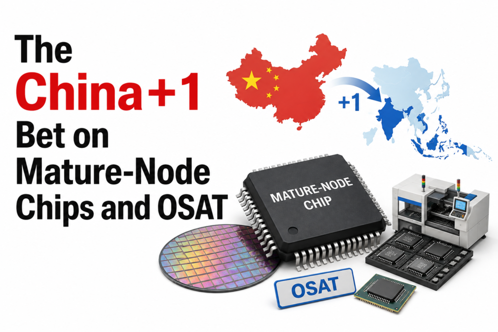
India isn’t trying to out-build Taiwan or South Korea on cutting-edge, sub-5-nanometer chips used in AI processors and flagship phones. That race requires decades of accumulated expertise and capital most countries simply don’t have. Instead, the strategy leans into what’s sometimes called a China+1 approach: courting companies that want a credible alternative to China for mature-node chips and assembly work, without necessarily leaving China behind entirely.
This is where outsourced semiconductor assembly and test, or OSAT, comes in. It’s the less glamorous, back-end part of chipmaking — taking finished wafers, cutting them into individual dies, packaging them, and testing them before they ship. It needs far less capital than building a wafer fab from scratch, which makes it a realistic entry point. China currently commands more than a third of the global OSAT market, with costs that run 10 to 30 percent lower than rivals thanks to sheer scale. India’s OSAT and assembly-testing-marking-packaging players are collectively pouring in several billion dollars, roughly half of it backed by government subsidy, to chip away at that lead. The pitch to global electronics brands isn’t just about price — it’s about not having all their eggs in one geopolitical basket.
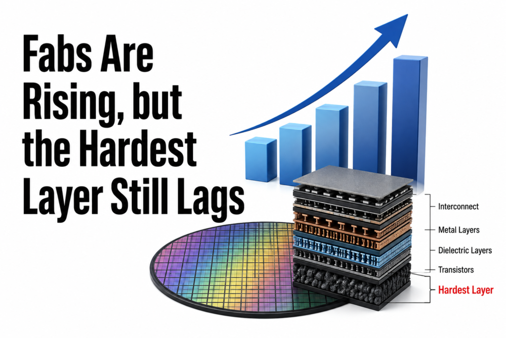
Fabs Are Rising, but the Hardest Layer Still Lags
The headline project remains Tata Electronics’ wafer fabrication plant in Dholera, built with Taiwan’s Powerchip Semiconductor. When it comes online, expected around 2028, it will be India’s first true silicon fab. The opening process node has slipped from the 28-nanometer target first announced to a more conservative 90 nanometers, a gap that hasn’t been fully explained publicly but reflects how difficult it is to stand up advanced fabrication from a standing start.
Even once that fab is running, it will depend almost entirely on imported lithography systems, deposition and etch tools, and specialty materials from a handful of global suppliers. Building a domestic base in these areas — machines, chemicals, ultra-pure gases — is arguably harder than building the fab itself, because it requires deep manufacturing expertise accumulated over generations elsewhere. Semicon 2.0’s inclusion of equipment and materials as a funded category is an acknowledgment that chip sovereignty means more than owning a factory; it means owning the inputs too.
Design, Demand, and What Comes Next

Manufacturing gets the headlines, but design is where India already has genuine strength — decades of experience writing the logic that goes inside chips, even without owning the factories that make them. Semicon 2.0 extends support to design projects and start-ups working on applications like video surveillance, energy metering, satellite communication, and IoT devices, with dozens of proposals already approved for funding and access to industry-grade design tools.
Domestic demand is the other quiet advantage. Smartphones, electric vehicles, industrial equipment, and telecom gear are all consuming more chips every year inside India, giving the mission a captive market to build around before it has to win fully on the export front. Officials talk about India eventually ranking among the world’s top semiconductor nations; getting there will mean stringing together fabs, packaging plants, equipment makers, and design houses into one coherent chain rather than a set of disconnected wins.
None of this makes India a chip superpower overnight, and nobody close to the programme is pretending otherwise. What Semicon 2.0 represents is a more honest, layered attempt at the problem — one that treats mature-node manufacturing, packaging, equipment, and design as pieces of a single puzzle instead of separate, disconnected wins. The plants opening this year are proof the mission can execute on paper commitments. Whether it can go the distance depends on the harder, less visible work still ahead: the machines, the specialty chemicals, and the years of patient, unglamorous investment that eventually turn early announcements into a durable industry other countries actually depend on.