



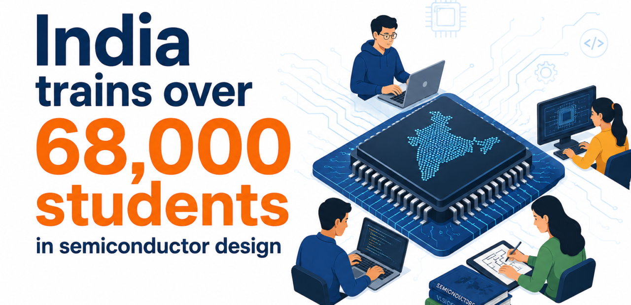
India Trains Over 68,000 Students in Semiconductor Design

A decade ago, almost nobody associated India with chip design. Today, a quiet revolution is underway — thousands of young engineers are learning to design, test, and tape out real semiconductor chips, and the numbers are finally catching up with the ambition. This shift didn’t happen overnight, and it isn’t slowing down anytime soon.
According to the Ministry of Electronics and Information Technology (MeitY), more than 68,000 aspiring chip designers have now been trained under the government’s Chips to Start-ups (C2S) Programme, with 254 chip designs already reaching the tape-out stage. It’s one of the clearest signs yet that India’s semiconductor ambitions are moving from paper to practice.
What Exactly Is the C2S Programme?

The Chips to Start-ups Programme was launched to solve a very specific problem: India had engineering talent, but not enough of it was trained in the highly specialised discipline of chip design. Designing a semiconductor isn’t like writing regular software — it requires exposure to industry-grade Electronic Design Automation (EDA) tools, an understanding of fabrication constraints, and hands-on practice that most college curriculums simply didn’t offer a few years ago.
C2S was built to close that gap. Its target is ambitious — creating 85,000 industry-ready professionals at the graduate, postgraduate, and doctoral levels who specialise in semiconductor chip design. Crossing the 68,000 mark means the programme is well past three-quarters of the way to that goal, and it has done so while keeping a strong focus on practical, real-world design experience rather than theory alone.
Importantly, the programme isn’t just about numbers of people trained. It’s built around giving learners access to the same tools used by professional chip design teams around the world, which is where the next part of the story gets interesting.
The Numbers Behind the Chip Design Push
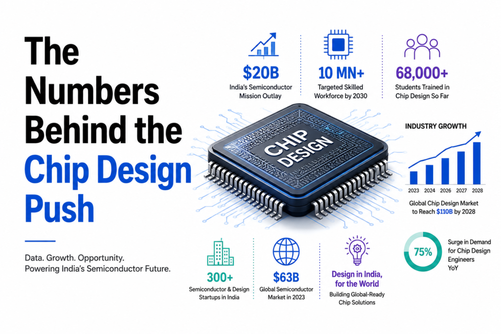
Training talent is only half the equation — the other half is giving that talent something real to work on. Under C2S, 332 academic institutions across the country have been given access to advanced EDA tools from major global players including Synopsys, Cadence, Siemens EDA, Ansys, Keysight, and Silvaco, among others. These are the same platforms used inside commercial chip design companies, not simplified academic versions.
That access has translated into tangible output. Of the 254 chip designs that have been taped out so far, 175 were completed at the 180 nanometre node using the Semiconductor Laboratory (SCL) in Mohali, while 79 more were taped out at semiconductor foundries overseas. Tape-out, for anyone unfamiliar with the term, is the final stage of chip design — the point where a completed layout is handed off to a foundry for actual manufacturing. Reaching tape-out is a meaningful milestone because it proves a design actually works well enough to be manufactured, not just simulated on a screen.
On top of that, EDA tool usage under the programme has already crossed 240 lakh hours, which gives a sense of just how much hands-on design work is happening across campuses rather than remaining confined to lectures and textbooks.
Building a Bigger Semiconductor Ecosystem

The C2S Programme doesn’t exist in isolation — it’s one piece of a much larger push under India’s Semicon 2.0 initiative, which was approved by the Union Cabinet with an outlay of roughly Rs 1.27 lakh crore. The broader goal is to build a complete domestic semiconductor value chain, covering everything from chip design to manufacturing, assembly, testing, and packaging.
Several supporting facilities have come up alongside the design training effort. A Skilled Manpower Advanced Research and Training (SMART) Lab has been set up at NIELIT Calicut, focused on Very Large Scale Integration (VLSI), embedded systems, and Internet of Things (IoT) training, and has already trained more than a lakh candidates. A new Semiconductor Assembly and Electrostatic Discharge Training Laboratory is also being established at NIELIT Guwahati, aimed at supporting the growing Assembly, Testing, Marking and Packaging (ATMP) ecosystem, particularly in India’s North Eastern region.
International collaboration is playing a role too. Agreements with universities like Purdue and Arizona State are expected to open doors for academic exchange, joint research, and greater exposure to global semiconductor practices. Separately, a partnership between the India Semiconductor Mission and Lam Research aims to train around 60,000 skilled professionals in nanofabrication and process engineering over the next decade — a sign that the talent pipeline is being built for manufacturing as much as for design.
Ongoing research projects at institutions in Andhra Pradesh, including work on a secure RISC-V processor at IIT Tirupati and hardware accelerators for high-performance computing at IIITDM Kurnool, show that the programme is also pushing toward original silicon research rather than just training on existing designs.
What It Means for Careers and the VLSI Job Market

For anyone tracking the VLSI and semiconductor job market in India, this milestone matters well beyond the headline number. A workforce trained on commercial-grade EDA tools and with real tape-out experience is directly employable by design houses, fabless semiconductor companies, and multinational chip firms setting up design centres in India. Employers no longer have to bridge as wide a gap between what fresh engineering graduates know and what a production design team actually needs.
It also signals where hiring demand is likely to grow. Companies expanding their India operations — whether in analog design, digital verification, physical design, or embedded systems — now have a larger, better-trained talent pool to recruit from, which could accelerate the pace at which global chip companies set up or scale design centres in the country. For those already working in VLSI or planning to move into it, the message is fairly clear: the ecosystem around them is maturing fast, and hands-on tool experience is becoming as valuable as a degree on paper.
India’s semiconductor story is still being written, and this training milestone is one of the more concrete chapters so far. With Semicon 2.0 backing continued investment, international collaborations widening, and thousands more expected to complete training in the coming years, the country’s push to become a genuine player in global chip design looks less like a policy goal and more like a work in progress that’s already showing results.