


Gujarat Boosts Chip Design with New Semiconductor Facility

Gujarat just made its boldest move yet in the race to become India’s chip design capital, and this time it isn’t about another factory floor. On August 7, 2026, the state government, Gujarat Technological University, and the Centre for Development of Advanced Computing kicked off a new Centre of Excellence built entirely around the art and science of designing chips.
For years, Gujarat’s semiconductor story has revolved around assembly lines and packaging units in places like Sanand and Dholera. This new initiative flips the script by putting design, the intellectual core of chip-making, at the center of the state’s strategy. Here is what the ChipIN Centre of Excellence in VLSI Design actually means for India’s semiconductor ambitions.
What Is the ChipIN Centre of Excellence in VLSI Design

The Gujarat State Electronics Mission, working under the Department of Science and Technology, has partnered with Gujarat Technological University and C-DAC Bengaluru to set up a ChipIN Extension Centre and Centre of Excellence focused on VLSI design. The kick-off meeting brought together experts from C-DAC Bengaluru, who walked participating institutions through the national ChipIN initiative and the tools it unlocks: Electronic Design Automation software, High Performance Computing resources, ready-to-use semiconductor intellectual property blocks, and, most importantly, tape-out support that lets a design actually get manufactured into silicon.
More than 30 institutions from across Gujarat showed up for the orientation, a strong early signal that the state’s academic and research ecosystem is hungry for this kind of infrastructure. Instead of designing a chip on paper and hoping to find a fabrication partner somewhere abroad, teams in Gujarat will now have a structured pathway to move from concept to a working prototype, all within the country.
Why Gujarat Is the Natural Base for a Design-Led Push

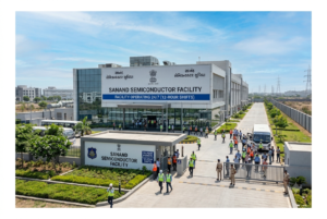
Gujarat already hosts the largest concentration of semiconductor manufacturing activity in India, including OSAT facilities in Sanand run by CG Semi, Kaynes Semicon, and Micron, alongside the Tata Electronics fabrication plant coming up in Dholera with ASML as a technology partner. Manufacturing capacity without local design capability is only half the picture, since chips still need to be architected before they can be assembled or fabricated.
By adding a dedicated design center to this mix, Gujarat is closing the loop between idea and product. A design team working near Sanand or Dholera can, in theory, take a concept through simulation, verification, and eventually tape-out without shipping the intellectual property overseas. This also gives startups and smaller companies in the state a realistic shot at building indigenous products rather than only serving as a manufacturing outpost for global chip brands. It is a shift from being a site on someone else’s map to becoming a place where original semiconductor ideas are born.
How This Fits Into India’s Broader Semiconductor Mission

The timing lines up with a larger national pivot. At the VLSI Design and Embedded Systems Conference held earlier this year, Indian officials spoke openly about moving from an assembly-heavy approach toward a product-led roadmap, one where the country designs its own chips rather than only testing and packaging chips designed elsewhere. Design hubs are already expanding in Noida and Bengaluru, targeting advanced process nodes, and Gujarat’s new center adds another serious player to that map.
This also connects to Semicon 2.0, the government’s expanded semiconductor push announced with a massive allocation spanning chip design, fabrication, and display manufacturing. The ChipIN network itself is a national program, so Gujarat’s extension center taps into shared infrastructure and expertise rather than starting from scratch. It is a smart way to scale design capability quickly without every state having to build identical, expensive infrastructure on its own.
What This Means for Careers and Skilling in Chip Design
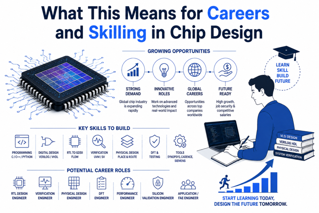
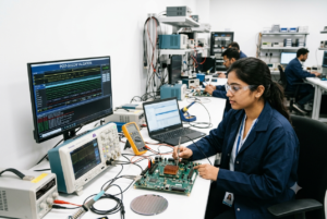
For anyone eyeing a career in semiconductor design, this development matters far beyond Gujarat’s borders. Access to real Electronic Design Automation tools, High Performance Computing resources, and tape-out support is exactly the kind of hands-on exposure that separates a strong chip design resume from an average one. Institutions plugged into the ChipIN network can now offer project work that mirrors what design engineers actually do in the industry, rather than staying limited to theory.
This growing emphasis on practical, tool-based training is also why demand for a structured VLSI course in Noida has picked up noticeably over the past year, as Noida itself is emerging as one of the advanced design hubs mentioned alongside Bengaluru. People considering such a course now have a clearer reason to enroll: the industry is actively building the infrastructure to absorb trained design talent, not just manufacturing talent. Whether someone trains in Gujarat, Noida, or elsewhere, the underlying message is the same. India’s semiconductor future needs people who can design chips, not only assemble them.