

Intel and Lens Technology Collaborate to Advance AI Semiconductor Packaging

What if the next leap in AI performance had nothing to do with faster processors, but with the material sitting quietly beneath them? Intel and Lens Technology have just announced a strategic collaboration built around exactly that idea, turning their attention to glass substrate packaging as a way to push AI hardware past its current physical and thermal limits.
This partnership brings together two very different kinds of expertise. Intel offers decades of chip architecture and advanced packaging know-how, while Lens Technology contributes precision glass manufacturing at massive industrial scale. Together, they are targeting one of the biggest bottlenecks in modern AI computing: how to package increasingly powerful chips efficiently and reliably.
What the Collaboration Actually Involves
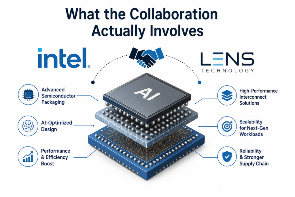
At the heart of this announcement is a shared effort to accelerate glass substrate-based packaging, a technology that replaces the traditional organic material used to connect and support chips with a more stable, precisely engineered glass base. Intel and Lens Technology plan to work jointly on through-glass via processes, a manufacturing method that creates tiny vertical connections through a glass panel, allowing signals and power to move between layers of a chip package with far greater accuracy than older approaches allow.
Under the arrangement, Intel is expected to focus on architectural design and verification, while Lens Technology takes the lead on precision processing and large-scale production of the glass substrates themselves. This division of labor plays to each company’s strengths: Intel understands how chips need to behave at the system level, and Lens Technology already runs the kind of high-volume, high-precision glass manufacturing that consumer electronics have relied on for years. Bringing those two skill sets together is what makes this collaboration meaningful rather than symbolic.
Why Glass Substrates Matter for AI Chips
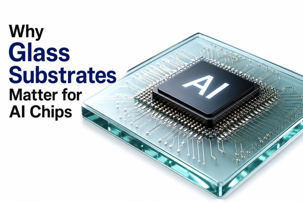
Glass substrates are not a cosmetic upgrade; they solve real engineering problems that have started to limit how far chip packaging can go. As AI workloads demand more compute packed into a single package, engineers need substrates that stay flat and stable under heat, allow denser and more precise wiring, and support better electrical performance across larger surface areas. Traditional organic substrates start to warp and lose precision at the sizes and densities modern AI chips now require.
Glass offers a more dimensionally stable alternative. It can support finer interconnects packed closer together, which directly increases the number of connections available in a given area. This translates into higher interconnect density, improved power delivery, and better thermal behavior, three factors that matter enormously for large AI accelerators and data center processors, where even small efficiency gains scale into significant real-world savings on power and cooling costs. For an industry racing to build ever-larger AI systems, packaging materials that can keep pace with chip design are no longer optional; they are becoming a competitive necessity.
Strategic Significance for Both Companies
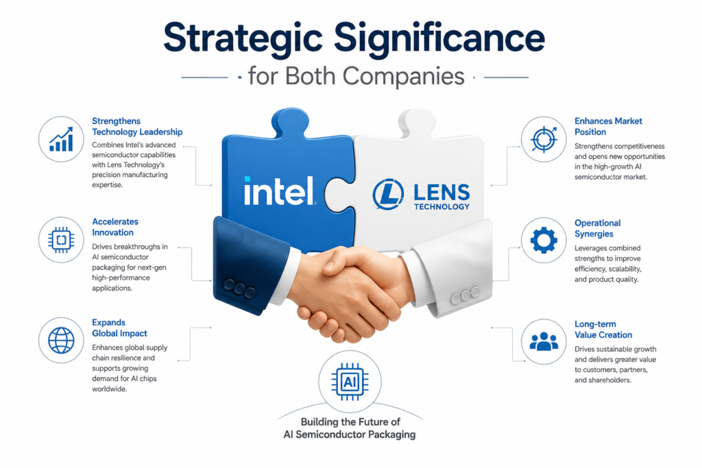
For Intel, this move fits into a broader strategy of strengthening its foundry and advanced packaging ecosystem at a time when competition in the space has intensified considerably. Rival chipmakers and foundries have been investing heavily in their own next-generation packaging approaches, and glass substrate technology has emerged as one of the more closely watched frontiers in that race. By partnering with an experienced manufacturing partner rather than building every capability internally, Intel gains a faster path toward maturing this technology.
For Lens Technology, the partnership represents something bigger than a single manufacturing contract. The company has built its reputation primarily through precision glass work for consumer electronics, and this collaboration marks a genuine step into the semiconductor materials supply chain. If through-glass via technology reaches successful commercialization, Lens Technology stands to gain a foothold in the advanced packaging substrate market, with room to grow into enterprise-level segments such as AI servers and data centers. It is a natural extension of existing expertise into a market with far higher long-term value.
What This Means for the Future of AI Computing

Beyond the core packaging work, both companies have signaled interest in exploring adjacent opportunities together, including components for AI PCs, structural and thermal solutions for data center hardware, and platforms supporting robotics and edge computing devices. None of these areas are guaranteed outcomes yet, but they point toward a broader vision: packaging innovation that supports AI not just inside massive data centers, but across a wider range of connected devices.
This kind of collaboration also reflects where the semiconductor industry is heading more broadly. As raw transistor scaling becomes harder and more expensive to achieve, packaging has increasingly become the place where meaningful performance gains still happen. Partnerships that combine chip design expertise with world-class materials manufacturing are likely to become more common, not less, as companies look for practical ways to keep pushing AI hardware forward.
It also highlights a shift in how global supply chains for advanced technology are forming. A company known for consumer glass manufacturing moving into semiconductor packaging shows how specialized industrial skills can cross over into entirely new markets when the underlying demand is strong enough. As AI infrastructure continues to expand at a rapid pace, this kind of cross-industry cooperation may become one of the more practical ways for the industry to keep up with demand, rather than every company trying to build every capability from scratch.
There is also a competitive angle worth noting. Other major players in the chip and foundry space have been exploring similar advanced packaging approaches of their own, which means this collaboration is as much about staying ahead as it is about pure technical innovation. Whoever manages to bring stable, high-volume glass substrate manufacturing to market first could gain a meaningful edge in supplying the next generation of AI hardware, from data center accelerators to AI-enabled edge devices.