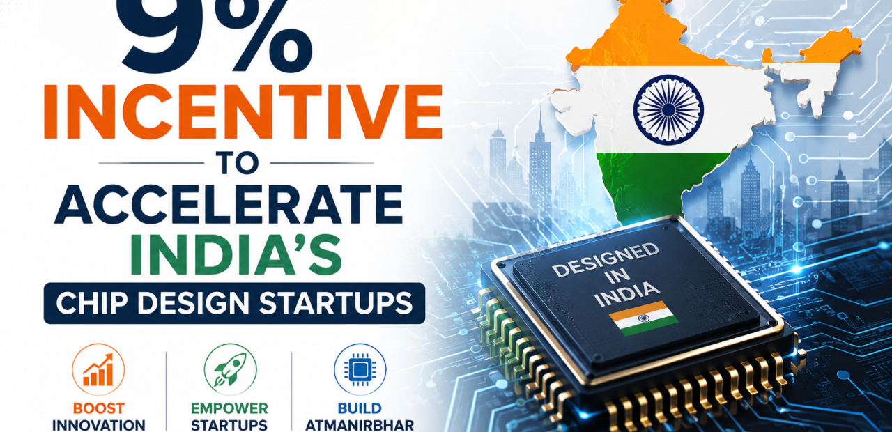
9% Incentive to Accelerate India’s Chip Design Startups

India has spent two decades designing chips for the rest of the world, quietly powering products it never gets to put its own name on. That is the uncomfortable part of the country’s semiconductor story. Now, a new 9% incentive is being lined up to change who actually owns the silicon India builds, and it could be the most important policy shift the domestic chip design industry has seen yet.
The plan targets one of the most expensive, least talked-about hurdles in chip design: turning a good idea into a working prototype. Fabricating that first chip at a commercial foundry can eat up a year and cost more money than most startups will ever raise, and this incentive is meant to close that gap so homegrown founders can compete on the same footing as global players.
What the 9% Deployment-Linked Incentive Actually Covers
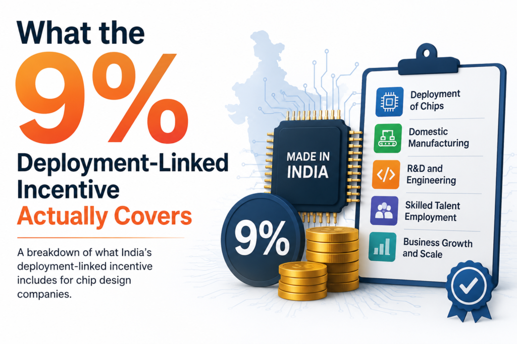
The India Semiconductor Mission is preparing to roll out a 9% deployment-linked incentive for domestic chip design startups under the proposed Semicon 2.0 programme. In plain terms, this incentive offsets the cost startups face when they take a chip design from paper to a physical prototype at a commercial foundry.
That step, known as tape-out and fabrication, is where most early-stage chip companies struggle. Large semiconductor companies negotiate volume discounts at foundries because they order in bulk. Startups don’t have that leverage, so they end up paying close to full price for a process that can already run into the hundreds of crores. The 9% incentive is designed to narrow that gap, effectively giving smaller design houses access to pricing that has historically only been available to bigger players.
Officials associated with the mission have described this as a deliberate move to keep chip design startups from stalling out right before their idea becomes a real, testable product. Prototyping is the point where many good designs die simply because there isn’t enough capital left to prove they work in silicon.
Why Prototype Costs Have Been the Real Barrier
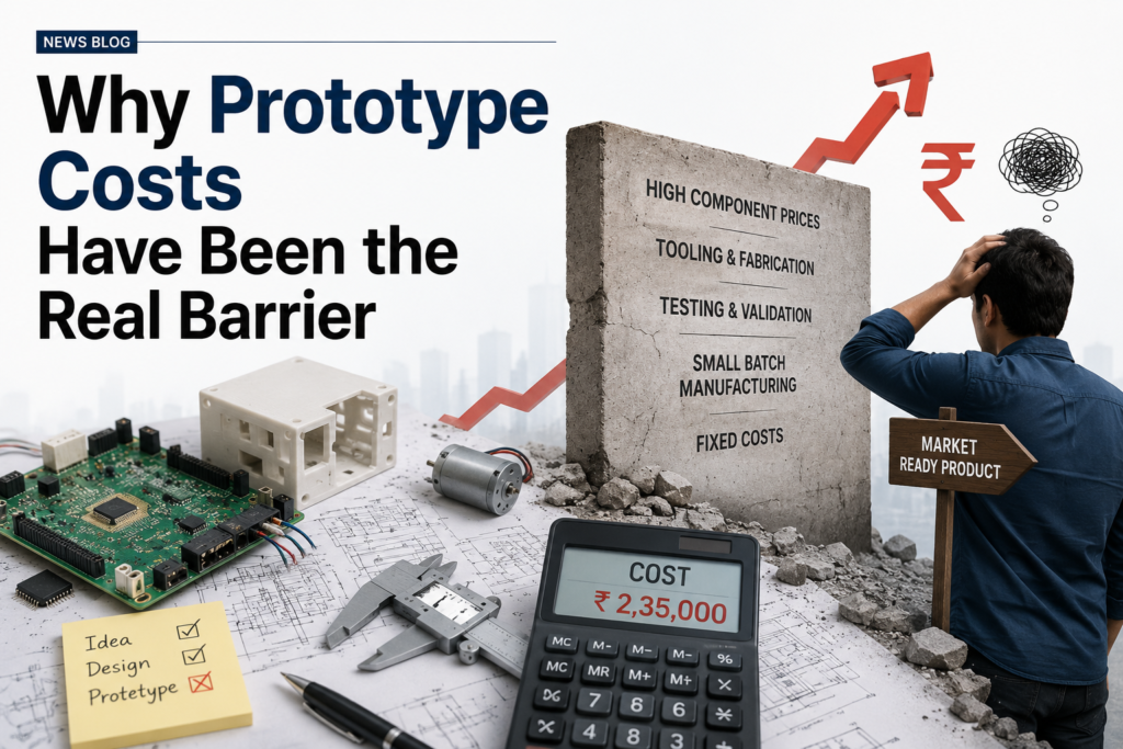
It’s easy to assume the hardest part of building a chip company is the design work itself, but the real wall has always been what comes after. Getting a prototype fabricated can take more than a year and, depending on the complexity of the chip, cost figures that run into thousands of crores. For a startup operating on limited runway, that single expense can decide whether the company survives long enough to bring a product to market.
This is also why India, despite having a massive base of chip design talent, has not yet produced a true design-led semiconductor unicorn. A handful of companies have come close, built largely on services and consulting work rather than owning proprietary chip IP. The gap has never really been about ideas or capability. It has been about the enormous capital required to move from a validated design to a chip that actually exists in the physical world. This new incentive is a direct response to that specific failure point.
Building on the Design Linked Incentive Scheme
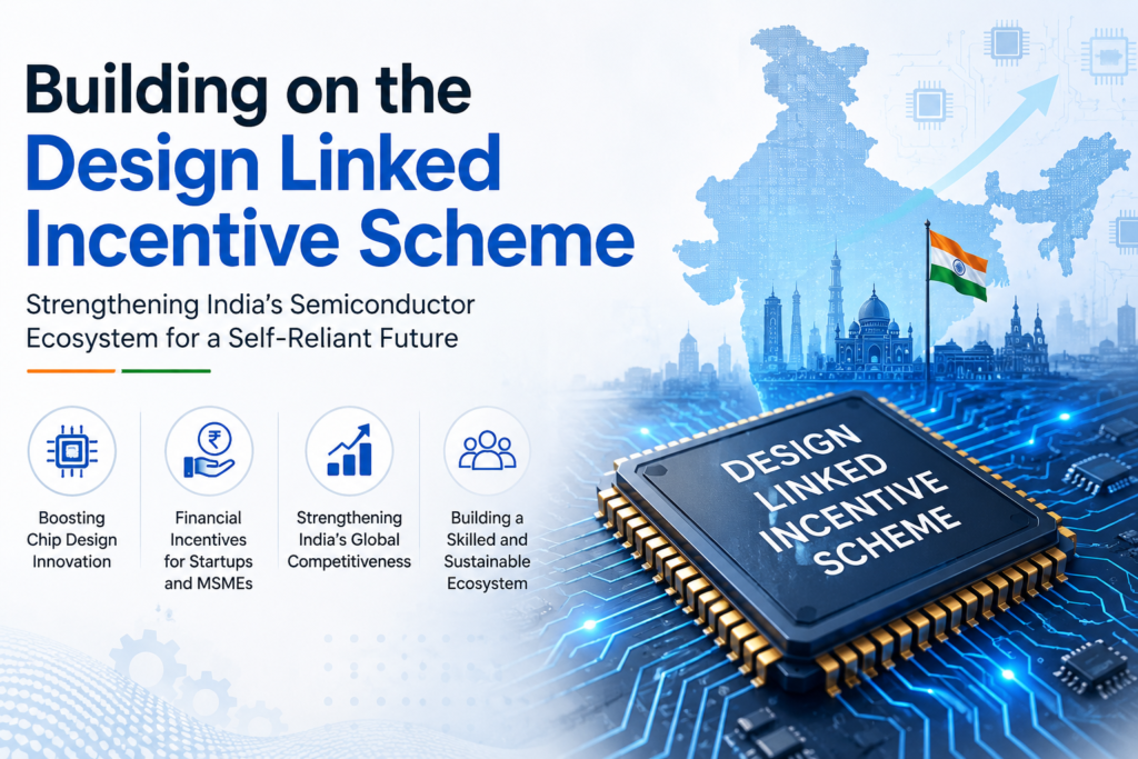
This isn’t happening in isolation. India already runs a Design Linked Incentive Scheme meant to support chip design companies through financial assistance and infrastructure support. That scheme has helped a growing number of startups move away from purely providing design services to third parties and start building and owning their own semiconductor intellectual property.
However, the funding caps under the earlier scheme were modest relative to how expensive prototyping has become. A support ceiling that made sense a few years ago simply doesn’t stretch far enough today, especially as chip designs get more complex and foundry costs keep climbing. The 9% incentive appears to be a recalibration of that support, built to match the real cost of getting a chip out of the design phase and into a lab where it can actually be tested.
Together, these two efforts point to a broader shift: after years of trying to attract manufacturing and packaging investment from abroad, the government’s incentive structure is stretching further backward into the design stage itself, which is arguably where India already has its strongest natural advantage.
What This Means for India’s Semiconductor Ambitions
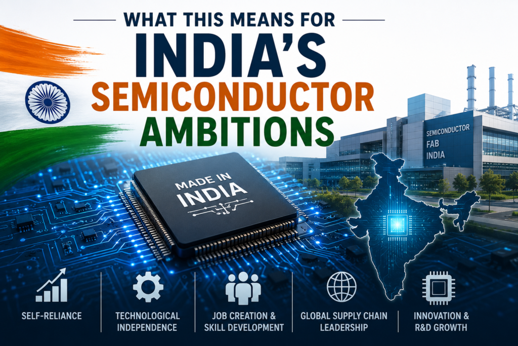
The timing matters. This incentive is expected to sit under the broader Semicon 2.0 programme, a large-scale second phase of the semiconductor mission that widens support across chip design, advanced packaging, equipment, and specialty materials rather than manufacturing alone. Domestic fabrication capacity is also expanding, with new fabs expected to come online in the next few years, which should eventually shorten the turnaround time startups currently lose to logistics and scheduling delays at overseas or third-party foundries.
For chip design startups, the practical impact could be significant. A lower prototyping cost means founders can take more design risks, iterate faster, and hold onto equity for longer instead of raising rounds purely to cover fabrication bills. It also changes the incentive structure for building original intellectual property instead of sticking to safer, services-based revenue models.
None of this guarantees India will produce a design-led chip unicorn overnight. Building a globally competitive semiconductor design company still depends on sustained investment, patient capital, and enough successful prototypes to build credibility with customers. But removing one of the biggest financial roadblocks in that journey is a meaningful step, and one that could shape how the next generation of Indian chip companies is built over the coming decade.
If this incentive rolls out as expected, it will be worth watching which startups move first to take advantage of it, and whether it finally produces the kind of design-owned success story India’s semiconductor ecosystem has been waiting for.