

N Channel vs P Channel MOSFET: Key Differences, Working & Applications

Flip a switch the wrong way in a power circuit and you don’t get a flicker — you get smoke. That’s the real-world stakes behind a question that sounds purely academic: should a design use an N channel or a P channel MOSFET? Get it wrong and a board fails on day one. Get it right and a product runs cooler, cheaper, and longer than its competitors.
This single choice quietly shapes everything from the phone charger on your desk to the battery management system in an electric scooter. Both transistor types do the same basic job — acting as an electronically controlled switch — but they get there through opposite physics, different strengths, and different failure points. Understanding that difference is what separates a circuit that works from one that just barely survives testing.
What a MOSFET Actually Does
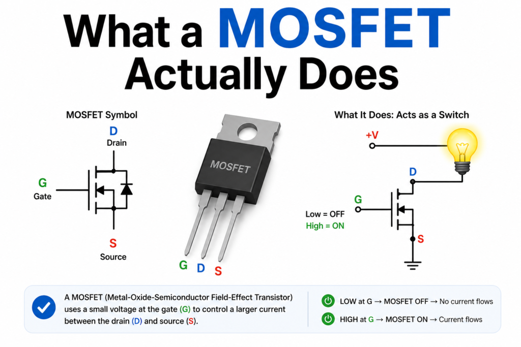
A MOSFET, short for Metal-Oxide-Semiconductor Field-Effect Transistor, is essentially a voltage-controlled gate for electric current. It has three main terminals — gate, drain, and source — and a small voltage applied to the gate decides whether current is allowed to flow between the drain and source. No moving parts, no mechanical wear, just an electric field doing the work of a switch.
Inside, the device is built on a silicon substrate with a thin insulating oxide layer under the gate. When the gate voltage crosses a certain threshold, it creates a conductive channel through the substrate, letting current pass. The nature of that channel — and what’s actually carrying the current through it — is exactly what separates the two families of MOSFETs.
N Channel MOSFET: How It Works
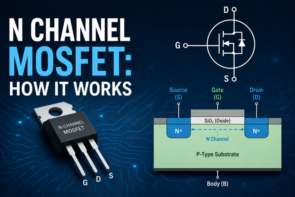
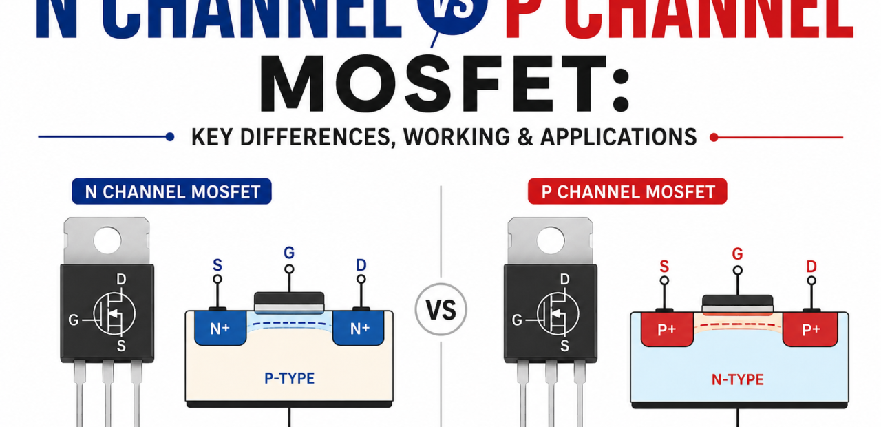
In an N channel MOSFET, the channel that forms is populated by electrons. Since electrons are the majority carriers here, turning the device on requires a positive voltage at the gate relative to the source. Once that threshold is met, electrons flow freely from source to drain, and the switch is effectively closed.
The reason N channel devices dominate the power electronics world comes down to one physical fact: electrons move roughly two to three times faster than holes through silicon. That higher mobility translates directly into lower on-resistance, which means less energy wasted as heat during conduction. For any application where efficiency and current-handling matter — DC-DC converters, motor drivers, switch-mode power supplies — this advantage is hard to ignore.
N channel MOSFETs are typically used for low-side switching, meaning they sit between the load and ground. This position suits their positive-gate-voltage requirement perfectly, since the gate drive circuitry can reference ground directly without needing extra components to generate a higher voltage.
P Channel MOSFET: How It Works
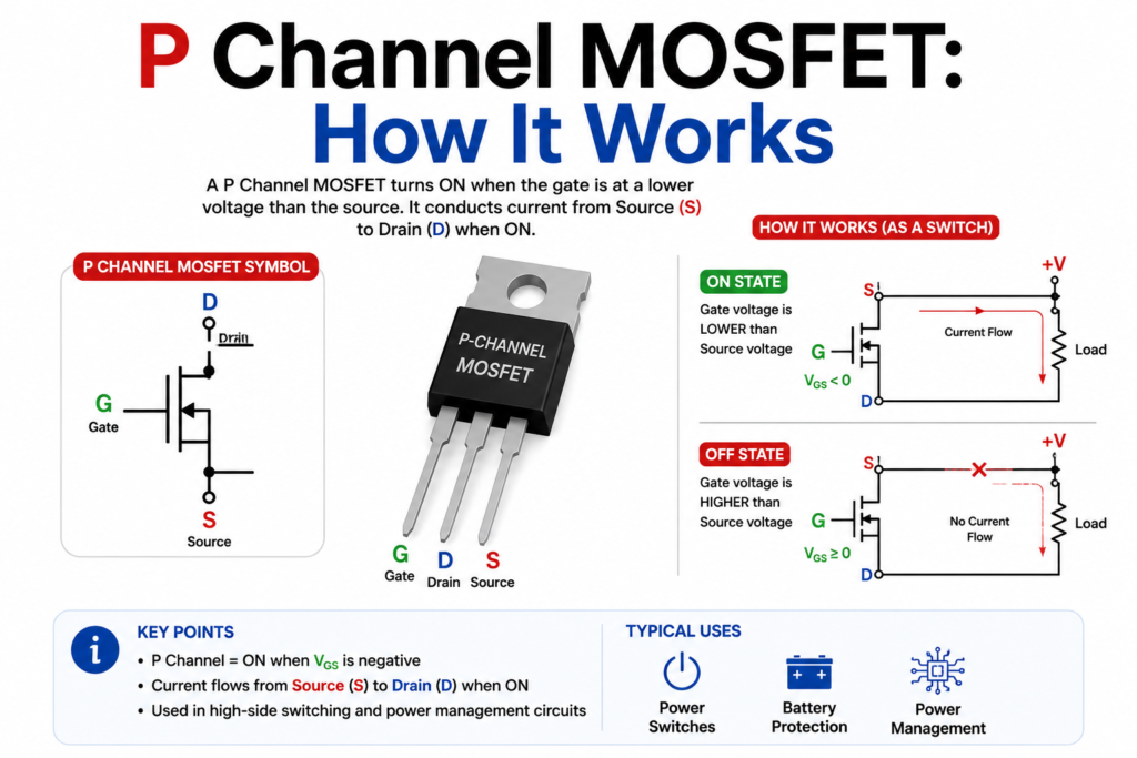
A P channel MOSFET flips the physics. Here, the channel conducts using holes — the absence of electrons that behaves like a positive charge carrier — and the device turns on when the gate voltage is negative relative to the source. Current then flows from source to drain in the opposite convention from an N channel device.
Because hole mobility is inherently lower than electron mobility, a P channel MOSFET needs a die roughly two to three times larger than an equivalent N channel part just to match the same on-resistance. That translates into higher cost per unit of current-handling capability and generally higher switching losses at high frequencies.
Where P channel devices earn their place is high-side switching, where the transistor sits between the power source and the load. In this position, driving an N channel device would require a charge pump or a bootstrap circuit to generate a gate voltage higher than the supply rail — extra parts, extra cost, extra complexity. A P channel MOSFET sidesteps all of that, since it can be switched on by simply pulling its gate below the source voltage using far simpler drive circuitry. This is exactly why P channel parts remain popular in low-power, low-voltage designs like battery protection circuits, load switches, and reverse-polarity protection, even though they lose ground in high-current territory.
Key Differences Between N Channel and P Channel MOSFETs
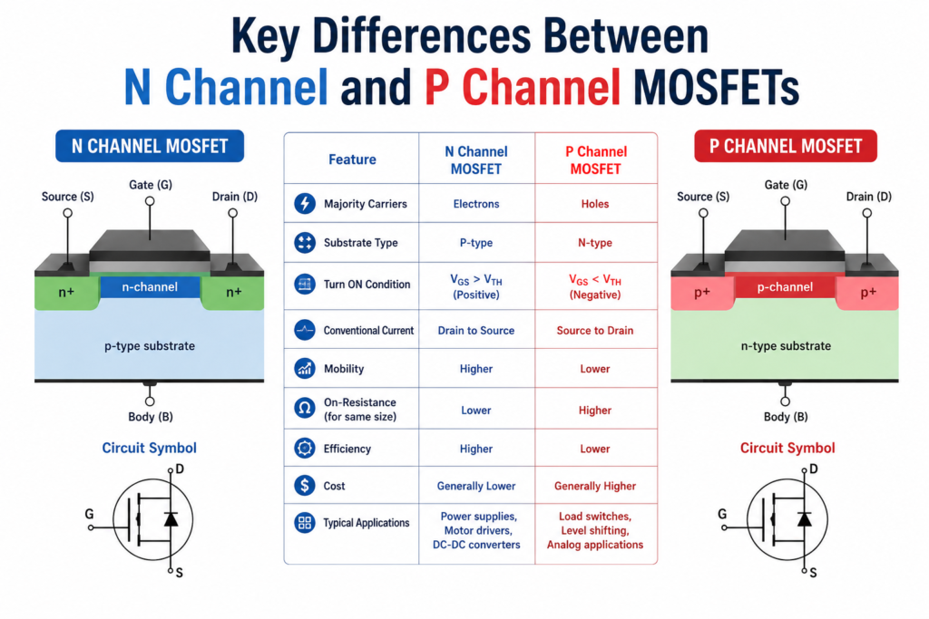
Laid side by side, a few contrasts stand out clearly.
Carrier type is the foundational difference — electrons in N channel devices versus holes in P channel devices — and this single fact cascades into every other distinction. On-resistance is lower in N channel MOSFETs because of superior carrier mobility, giving them a real edge in high-current, high-efficiency applications. Die size tells a similar story: matching performance forces P channel devices to be physically larger, driving up manufacturing cost.
Gate voltage polarity is the other major divide. N channel devices switch on with positive gate voltage and are naturally suited to low-side switching, while P channel devices need negative gate voltage and fit high-side switching without extra driver circuitry. Switching speed generally favors N channel MOSFETs too, since their smaller intrinsic capacitances allow faster transitions, which matters enormously in high-frequency power conversion.
None of this makes one type universally “better.” It simply means each was built to solve a different placement problem in a circuit, and swapping one for the other without redesigning the surrounding drive circuitry will cause the switch to fail or short outright — the two are not interchangeable, despite sounding like mirror images of each other.
Real-World Applications and Where the Industry Is Headed

N channel MOSFETs show up almost everywhere current needs to be handled efficiently: switch-mode power supplies, motor controllers, LED drivers using pulse width modulation, and the low-side switches inside laptop and EV chargers. Their fast switching also makes them a staple in RF amplifier stages and audio equipment where signal integrity at speed genuinely matters.
P channel MOSFETs, meanwhile, are the quiet workhorses of battery-powered devices. Load switches, reverse-battery protection circuits, and simple high-side power gating in portable electronics rely on them because the simplified gate drive saves board space and cost — details that matter enormously at scale.
There’s also a bigger structural shift underway. As power electronics push toward higher voltages and tighter thermal budgets — driven by everything from AI data center power delivery to 48V automotive systems — wide-bandgap materials like silicon carbide and gallium nitride are increasingly used alongside or instead of traditional silicon MOSFETs. These newer devices push efficiency and switching speed further, but the underlying N-type versus P-type logic that governs silicon MOSFETs still shapes how engineers think about channel selection even in these advanced designs. And in nearly all of them, the complementary pairing of N channel and P channel devices inside CMOS technology remains the backbone of low-power digital logic, balancing speed and near-zero static power draw.
Conclusion
The decision usually comes down to where the switch sits and how much current it needs to carry. For low-side switching in anything demanding efficiency at meaningful current levels, N channel is almost always the default choice. For high-side switching in low-power or battery-conscious designs where simplicity of the gate drive outweighs raw efficiency, P channel earns its spot.
A quick gut check often helps during the design phase: if the switch needs to handle serious current with minimal heat loss, and it sits on the ground side of the load, N channel is the natural fit. If the switch sits on the supply side, current levels are modest, and simplifying the driver circuit matters more than squeezing out every last bit of efficiency, P channel usually wins. Datasheets are worth reading closely too — comparing on-resistance, gate charge, and voltage ratings between candidate parts often reveals a clearer answer than theory alone.
Rather than treating this as a rivalry, it’s more useful to see N channel and P channel MOSFETs as complementary tools, each solving a distinct half of the switching puzzle. Knowing when to reach for which one — rather than defaulting to whichever is more familiar — is what separates a well-engineered power design from one that just happens to work on the bench.
1. What is the difference between N Channel and P Channel MOSFET?
N Channel MOSFETs use electrons for faster switching, while P Channel MOSFETs use holes, making them ideal for high-side switching and simpler circuit designs.
2. Which MOSFET is better, N Channel or P Channel?
N Channel MOSFETs offer lower resistance and higher efficiency, while P Channel MOSFETs are preferred for high-side switching in many electronic circuits.
3. Where are N Channel MOSFETs used?
N Channel MOSFETs are widely used in SMPS, motor drivers, inverters, DC-DC converters, battery systems, and high-speed switching applications.
4. What are the applications of P Channel MOSFET?
P Channel MOSFETs are commonly used in load switches, battery protection circuits, power management, reverse polarity protection, and high-side switching.
5. Why is N Channel MOSFET faster than P Channel?
Electrons have higher mobility than holes, allowing N Channel MOSFETs to switch faster and deliver better performance with lower power losses.