

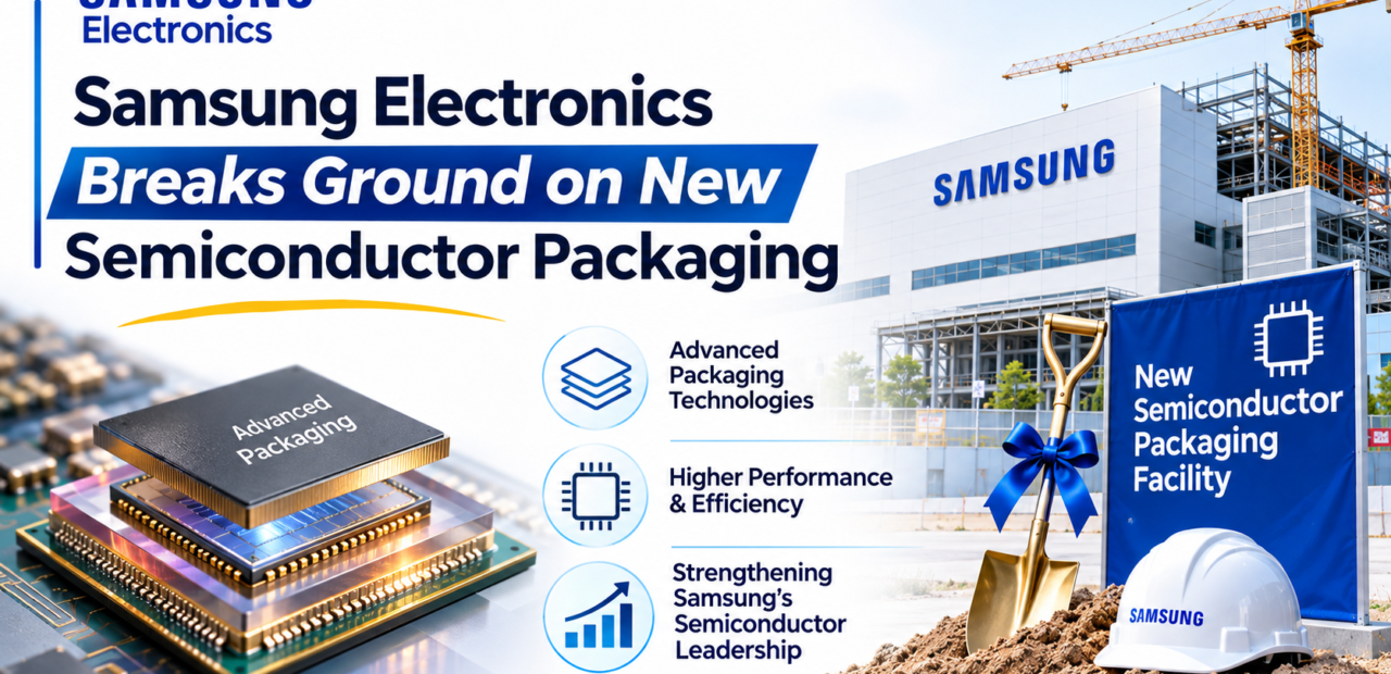
Samsung Electronics Breaks Ground on New Semiconductor Packaging

The semiconductor industry is entering a new phase of technological development, driven by the growing demand for artificial intelligence, high-performance computing and advanced data processing. As AI applications become more complex, chip manufacturers are focusing not only on improving processor performance but also on developing more efficient memory architectures and packaging technologies. In an important industry development, Samsung Electronics has officially broken ground on a new advanced semiconductor packaging facility at its Onyang campus in Asan, South Korea. The project represents a strategic investment in High-Bandwidth Memory (HBM) technology, which plays an essential role in modern AI infrastructure.
The new facility is expected to strengthen Samsung’s advanced packaging capabilities and support the growing requirements of next-generation AI semiconductor systems. The groundbreaking ceremony took place on November 12, 2026, with South Korean President Lee Jae-myung and Samsung Electronics Executive Chairman Lee Jae-yong in attendance. Samsung plans to develop the Onyang campus into an important production hub for advanced HBM packaging. With substantial investments planned for factory infrastructure and manufacturing equipment, this development highlights how semiconductor manufacturing is evolving beyond traditional fabrication processes. It also demonstrates the increasing importance of packaging technology in the global VLSI ecosystem.
Samsung’s New Semiconductor Packaging Facility: Project Overview
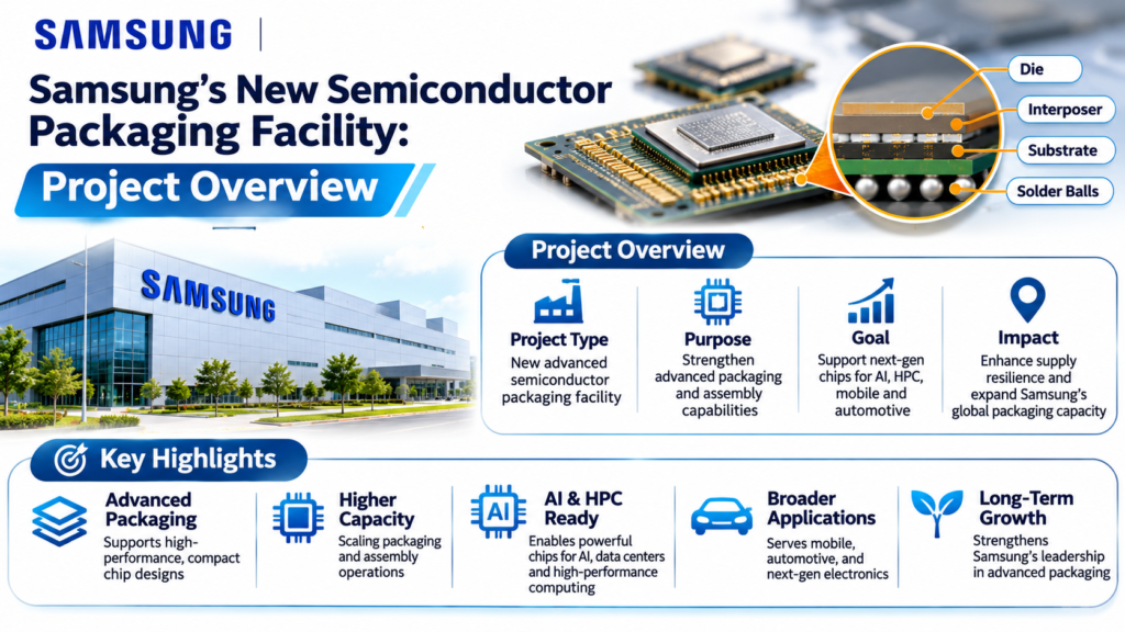
Samsung Electronics has started construction of a new advanced semiconductor packaging facility at its Onyang campus in Asan, South Korea. The development is part of a broader investment strategy aimed at strengthening the company’s semiconductor manufacturing capabilities and expanding its position in the AI memory market.
The overall investment plan for the Onyang expansion is approximately 46 trillion Korean won, including around 6 trillion won for the facility and 40 trillion won for advanced equipment. The expansion includes plans for five HBM production lines, with the new production facility expected to begin operations in June 2028.
Why Advanced Packaging Is Important for HBM Technology
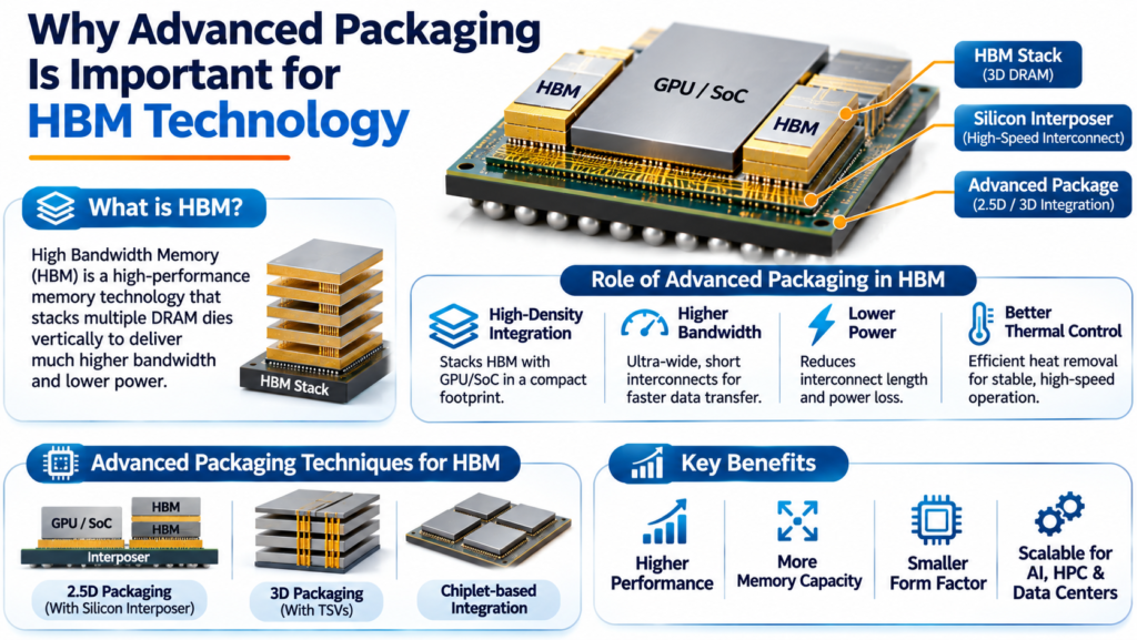
High-Bandwidth Memory is a specialized memory technology designed to deliver high data transfer rates and support demanding computing workloads. It achieves this through vertically stacked DRAM dies connected using advanced interconnection technologies. This architecture allows processors to access large amounts of data efficiently.
Advanced packaging plays a critical role in making HBM products possible. Processes such as die stacking, bonding, interconnection and thermal management require highly precise manufacturing techniques. As AI processors demand greater memory bandwidth and efficiency, improvements in packaging technology are becoming increasingly important for semiconductor manufacturers.
How the New Facility Supports AI Semiconductor Manufacturing
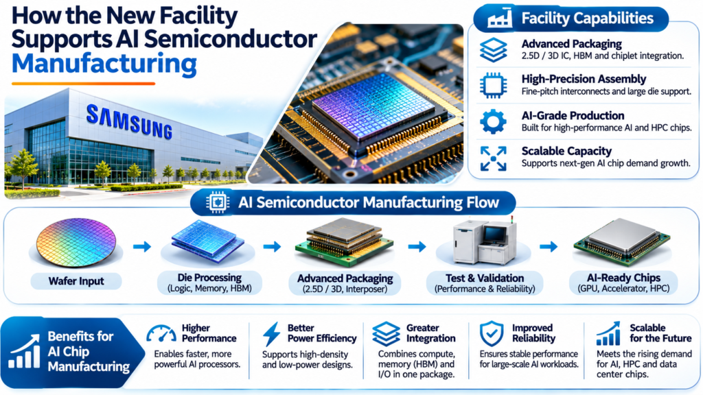
Artificial intelligence applications require significant computing resources, particularly when processing large datasets and training complex machine learning models. GPUs and AI accelerators depend on high-performance memory systems to transfer information quickly between processing units and memory components.
Samsung’s investment in advanced HBM packaging is intended to strengthen this important part of the semiconductor supply chain. Increasing packaging capacity can help improve the availability of finished HBM products while supporting the development of more advanced memory solutions. The new facility also reflects the industry’s growing focus on integrating memory and processing technologies to meet future AI computing requirements.
Advanced Semiconductor Packaging vs Traditional Packaging
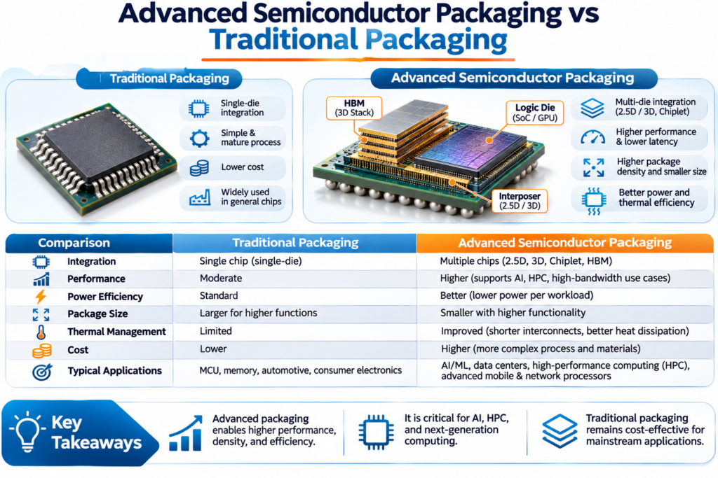
Traditional semiconductor packaging primarily focuses on protecting individual semiconductor dies and providing electrical connections between the chip and the external system. These approaches have supported conventional processors, memory devices and electronic components for many years.
Advanced packaging introduces more sophisticated integration techniques, including multiple-die arrangements, vertical stacking and high-density interconnections. These capabilities make it possible to develop compact semiconductor systems with higher bandwidth and improved integration. Samsung’s new facility highlights the industry’s transition towards advanced packaging solutions that support demanding AI and high-performance computing applications.
| Comparison Factor | Traditional Packaging | Advanced Semiconductor Packaging |
|---|---|---|
| Chip arrangement | Generally individual dies | Multiple dies and stacked structures |
| Interconnections | Conventional bonding methods | High-density interconnections |
| Data transfer | Depends on package architecture | Supports higher-bandwidth integration |
| Integration | Comparatively limited | Greater system integration |
| Manufacturing complexity | Relatively established processes | More sophisticated processes |
| Applications | General-purpose electronics | AI accelerators, HBM and HPC systems |
What Samsung’s Investment Means for the Future of VLSI
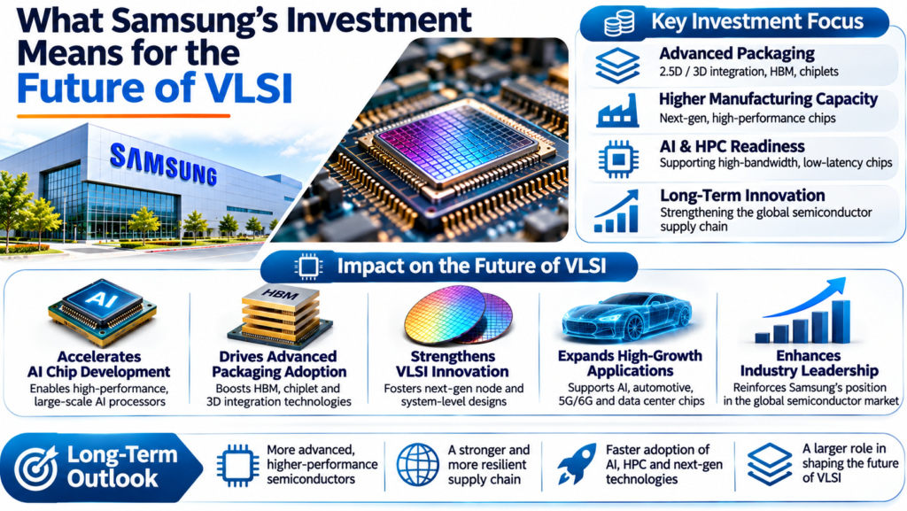
Samsung’s new packaging facility represents an important development for the future of Very Large Scale Integration (VLSI). As semiconductor devices become smaller and more complex, improving transistor performance alone is no longer sufficient to meet every computing requirement. Designers and manufacturers are increasingly exploring advanced packaging, chiplet integration and heterogeneous integration to improve overall system performance.
This development could also create new opportunities across the semiconductor ecosystem, including packaging process development, physical design, thermal analysis, signal integrity and semiconductor testing. For VLSI engineers, understanding both front-end chip design and back-end packaging processes will become increasingly valuable as the industry moves towards more integrated semiconductor architectures.