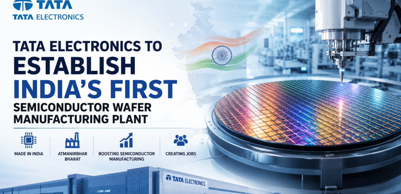
Tata Electronics to Establish India’s First Semiconductor Wafer Manufacturing Plant

For decades, India designed the chips the world uses but never made them at home. That changes now. A 600-acre stretch of land in Dholera, Gujarat, is turning into the site of the country’s first commercial semiconductor wafer fabrication plant, and the company behind it is a name most Indians already trust from a completely different industry: Tata.
Tata Electronics has partnered with Taiwan’s Powerchip Semiconductor Manufacturing Corporation (PSMC) to build this facility, backed by an investment of roughly ₹91,000 crore. It’s not a small pilot project or an assembly unit — it’s a full-scale wafer fab, the kind of plant that takes raw silicon and turns it into the chips running everything from cars to smartphones to industrial equipment. This blog breaks down what’s actually being built, who’s involved, when it will start producing chips, and why it matters for India’s electronics future.
Inside the Dholera Fab: Scale, Investment and Technology
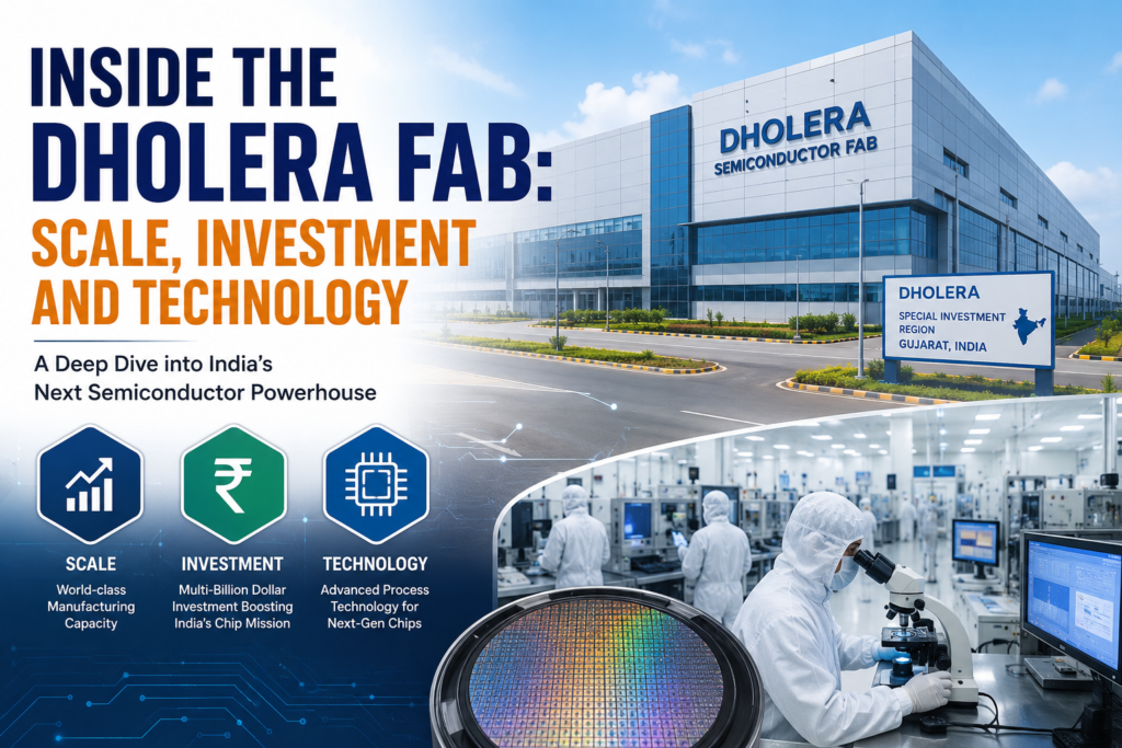
The Dholera plant is designed to produce around 50,000 wafers per month once fully operational, placing it firmly in the league of serious global foundries rather than a token manufacturing effort. The facility will focus on chips built on 28, 50, and 55-nanometer process nodes — not the bleeding-edge nodes used in flagship smartphone processors, but exactly the nodes that power the products India actually needs at scale: power management ICs, display driver chips, microcontrollers, and high-performance compute chips for automotive and industrial use.
That focus is deliberate. Rather than chasing the most advanced (and most expensive) chip technology in the world on day one, Tata Electronics and PSMC are targeting the segment where demand is enormous and currently almost entirely import-dependent — automotive electronics, consumer devices, telecom equipment, and defense applications. Building expertise here first gives India a realistic entry point into a notoriously difficult industry, with room to move toward more advanced nodes in later phases.
The Gujarat government has also been developing residential and civic infrastructure around the site, since a project of this scale draws thousands of skilled workers and their families to what is essentially a new industrial township taking shape around the fab.
The ASML Partnership: Bringing World-Class Lithography to India
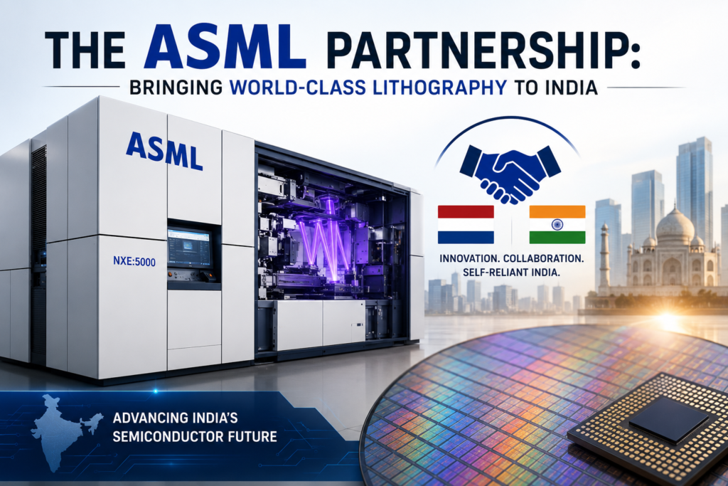
No modern chip fab can function without lithography — the precise, almost impossibly exact process of etching circuit patterns onto silicon wafers. This is where ASML, the Dutch company that effectively controls the global supply of advanced lithography machines, enters the picture.
Tata Electronics signed an agreement with ASML to supply lithography tools and solutions for the Dholera fab, a deal formalized in the presence of top government officials from both India and the Netherlands. Given that lithography scanners typically take 18 to 24 months to deliver from order to installation, locking in this partnership early was essential to keeping the fab’s production timeline realistic.
This collaboration matters beyond just equipment supply. It signals that a company at the very center of the global chip supply chain sees enough long-term potential in India’s semiconductor push to commit its most advanced technology here — at a time when many countries are competing hard to diversify chip manufacturing away from a handful of existing hubs.
From Groundbreaking to First Chip: The Production Timeline
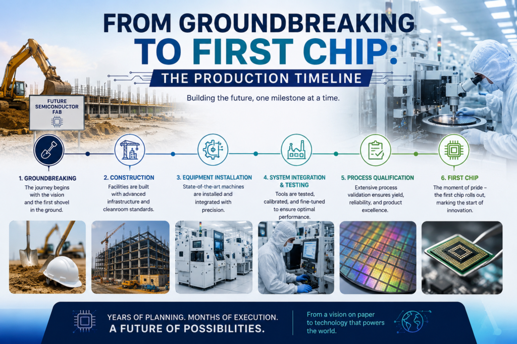
Construction on the Dholera fab has progressed steadily, crossing roughly the halfway mark by the middle of 2026. Trial production is expected to begin around December 2026, with a gradual ramp toward full commercial-scale output through 2027 and into 2028 as the plant works its way up to its target capacity of 50,000 wafers per month.
This phased approach is standard for an operation this complex. Trial runs allow engineers to calibrate fab equipment, validate process quality, and iron out issues before scaling up — a critical step given how unforgiving chip manufacturing is to even microscopic defects. A supporting ecosystem is also forming alongside the main fab; specialty gas suppliers, for instance, are setting up nearby facilities to provide the ultra-high-purity gases that wafer fabrication depends on, which is often a strong sign that a manufacturing hub is maturing rather than existing in isolation.
Why This Plant Matters for India’s Electronics Ecosystem
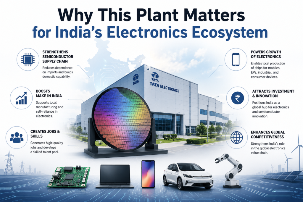
India currently ranks among the largest importers of semiconductor chips in the world, relying heavily on the United States, Japan, and Taiwan to meet its demand. Every smartphone, car, and appliance assembled in India today still depends on chips manufactured somewhere else. A domestic wafer fab changes that equation in a way that assembly and packaging plants alone cannot.
The Dholera project isn’t happening in isolation either. Around the same time, Tata Electronics has been running an assembly and test facility in Jagiroad, Assam, and other companies have been setting up their own packaging and testing units across states like Gujarat and Rajasthan. Together, these projects represent India’s broader attempt to build a complete semiconductor value chain — from raw wafer to finished, packaged chip — rather than depending on a single link of that chain.
For automotive manufacturers, defense contractors, and consumer electronics brands operating in India, a reliable domestic source of these chips could mean shorter supply chains, lower exposure to global shortages, and faster access to components tailored for local needs. It also positions India as a genuine alternative in a global semiconductor map that has long been concentrated in just a few countries.