


HCL Technologies Limited (HCLTECH) Launches India Centers for Rapidus Semiconductor Work

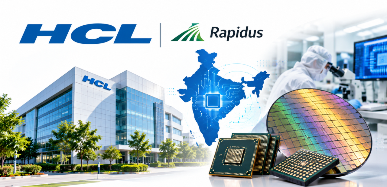
The global semiconductor landscape is witnessing a structural shift as demand for advanced logic chips continues to accelerate rapidly. In a major strategic development within the VLSI industry, HCL Technologies Limited (HCLTECH) has announced the opening of two dedicated offshore development centers in India to support Japan-based Rapidus Corporation. Situated in Bengaluru and Hubli, these modern facilities are engineered to handle cutting-edge semiconductor design and technology co-optimization workflows, positioning India as a key global nerve center for next-generation silicon engineering.
This high-value partnership highlights the deepening technology corridor between India and Japan while addressing critical talent bottlenecks in advanced chip design. By leveraging HCLTech’s deep domain expertise in core engineering, physical design, and infrastructure automation, Rapidus aims to compress product development lifecycles for complex logic semiconductors. For the Indian engineering ecosystem, this initiative opens up high-skilled VLSI jobs while reinforcing the country’s ongoing shift from purely software operations to high-end hardware and semiconductor R&D.
Expanding Silicon Design Facilities in Bengaluru and Hubli
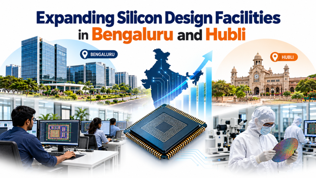
The inauguration of new development centers across Bengaluru and Hubli marks an expansive operational step for HCLTech’s semiconductor engineering vertical. While Bengaluru provides access to an established ecosystem of microelectronics engineers, the Hubli center underlines an emerging industry trend of expanding high-tech hardware research into tier-2 Indian cities. Together, these hubs will host specialized teams tasked with delivering complex tape-out support, advanced physical layouts, and physical verification pipelines essential for sub-nanometer fabrication targets.
By deploying specialized engineering teams across both locations, HCLTech offers Rapidus scalable R&D capacity without compromising execution speed or technical consistency. The Hubli development center, in particular, offers strategic advantages in talent retention and operational resilience, creating a balanced delivery model. As semiconductor node scaling becomes increasingly challenging, having dual-location support in India equips Rapidus with continuous, round-the-clock engineering cycles vital for complex VLSI tape-outs.
Core Technical Domains: PDK, DTCO, and Mask Design
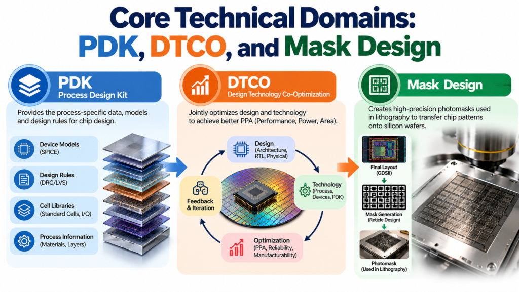
Under this collaborative roadmap, HCLTech will execute complexVLSI tasks crucial for modern foundry operations. The engineering scope spans Process Design Kit (PDK) development, Design Technology Co-Optimization (DTCO), layout design, mask design, and custom infrastructure setups. PDK development serves as the essential bridge between manufacturing foundries and chip designers, ensuring that design rule manuals and simulation models accurately reflect real-world process variations at advanced fabrication nodes.
Design Technology Co-Optimization (DTCO) plays an equally vital role by simultaneously optimizing transistor architecture and physical design layouts. Through tight DTCO execution, HCLTech engineers will help Rapidus maximize power, performance, and area (PPA) metrics before committing to expensive mask creation. Combined with precision mask layout engineering, these technical efforts significantly reduce iteration delays, lower fabrication risks, and enable smooth production scaling for next-generation logic chips.
Strategic Impact on the India-Japan Technology Corridor
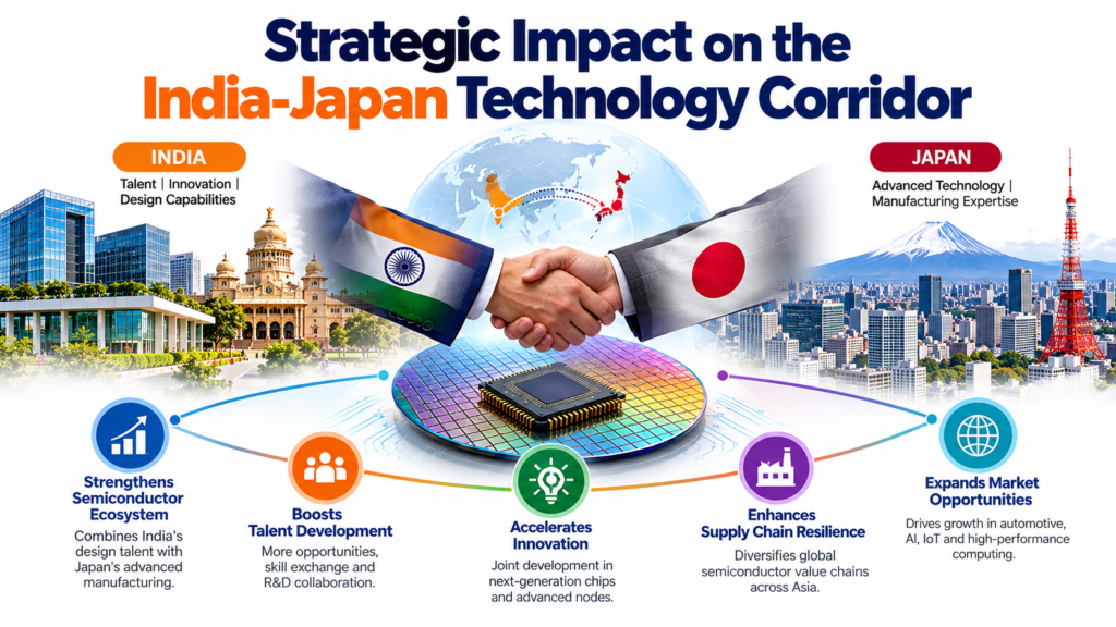
This joint enterprise represents more than a standard commercial contract; it builds upon growing technological and economic alignment between Japan and India. As Japan accelerates efforts to rebuild its domestic advanced semiconductor manufacturing foundation through Rapidus, partnering with Indian technology leaders secures the specialized human capital required for ambitious execution timelines. The engagement establishes a direct bridge for technical knowledge sharing between two prominent technology hubs.
Furthermore, the collaboration includes structured initiatives to construct a long-term talent pipeline, preparing Indian chip designers for specialized roles within Japan’s evolving semiconductor landscape. As multinational tech companies continuously restructure supply chains for resilience, bilateral engagements like the HCLTech-Rapidus initiative establish reliable frameworks for joint hardware innovation, IP creation, and international talent mobility.
Transforming India’s Tier-2 Cities into Semiconductor Hubs
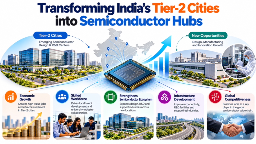
Establishing high-end VLSI development facilities in regional centers like Hubli demonstrates the decentralized growth of India’s technology sector. Historically concentrated in metropolitan areas, advanced chip design operations are progressively expanding outward as regional engineering institutions mature and infrastructure improves. This shift reduces operational concentration while providing skilled engineers with opportunities to work on cutting-edge technology outside tier-1 metros.
The Hubli setup offers a clear model for expanding high-value R&D operations across secondary cities. By supporting this facility alongside the primary hub in Bengaluru, HCLTech demonstrates that complex engineering functions—including PDK verification and physical design layout—can operate seamlessly across distributed geographical centers. This trend enhances India’s overall capacity to support global semiconductor demand.
Accelerating Time-to-Market for Next-Gen Logic Chips

In the semiconductor industry, reaching market availability early is critical to commercial viability. By offloading resource-intensive physical design, PDK calibration, and verification tasks to HCLTech’s dedicated centers, Rapidus can focus on core architecture and fabrication processes. This division of labor helps shorten development cycles for complex logic chips targeted at artificial intelligence, high-performance computing, and automotive electronics.
The integration of automated layout methodologies, specialized scripts, and robust verification flows ensures high precision across all stages. As logic nodes continue to scale downward, early error detection in physical design prevents costly resubmissions during mask fabrication. The dedicated technical centers provided by HCLTech furnish the dedicated capacity needed to maintain rigorous quality control while adhering to strict project deadlines.