


Why India is best place to Start your VLSI Career

Picture a chip smaller than a fingernail, designed on a laptop in Bangalore, that ends up running inside a car in Germany or a smartphone in Seoul. That is not a distant dream anymore, it is already happening today. India has quietly turned into one of the most exciting places on earth to build a long-term career in chip design, and the momentum behind it shows no signs of slowing down anytime soon.
For decades, India was known mainly for supporting the world’s chip industry from behind the scenes. That story is changing fast. Government-backed fabrication plants, billion-dollar investments, and a wave of new design centres mean fresh opportunities are opening up faster than almost anywhere else in the world. If you are trying to figure out where to build a lasting career in semiconductor design, here is why India genuinely deserves a serious look.
1. A Semiconductor Mission That Is Actually Delivering
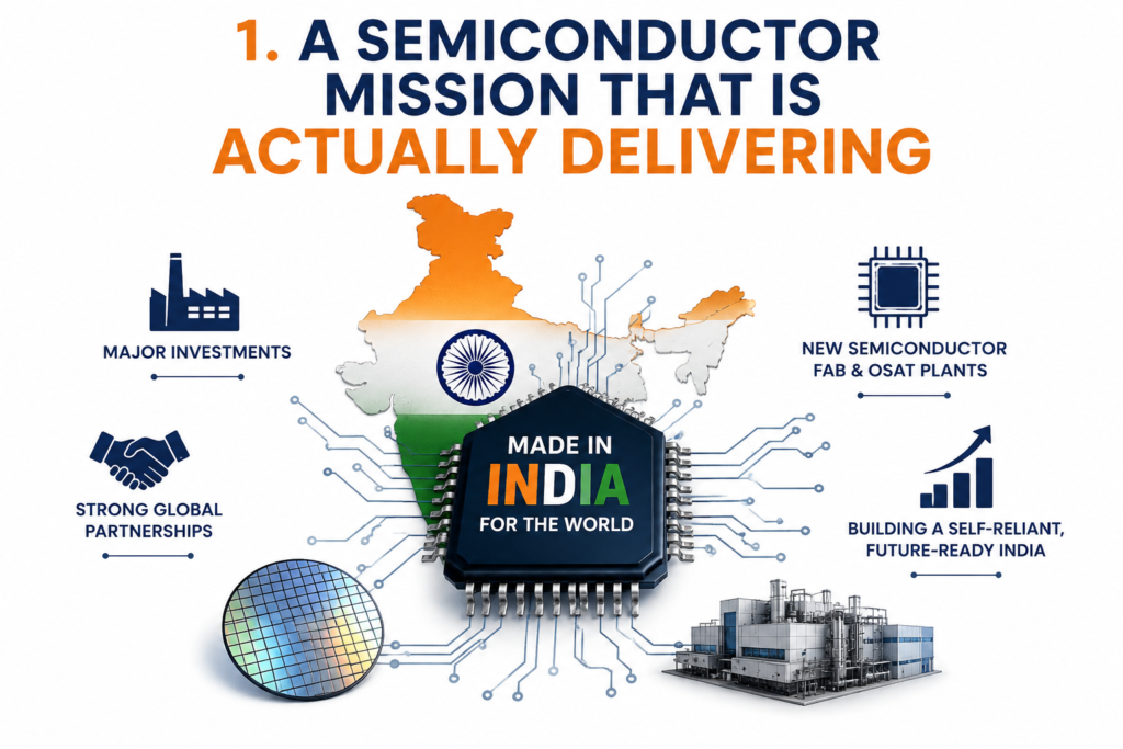
For years, India talked about becoming a chip-making powerhouse. In 2026, that talk has turned into concrete progress. The India Semiconductor Mission has pushed billions of rupees into new fabrication facilities, packaging plants, and design incubators across the country. Major projects, including the Tata Electronics facility in Gujarat, are moving from groundbreaking ceremonies to actual production timelines.
What makes this shift meaningful for a career is the sheer range of roles it creates. It is no longer just about writing code for someone else’s chip design abroad. Engineers in India are now involved in end-to-end product development, from architecture and RTL design to verification, physical layout, and packaging. This “product-led” push means the work is becoming more ownership-driven, more visible, and more rewarding than the outsourced service model of the past.
2. Global Companies Are Building Deep Roots Here

Nearly every major chip company on the planet already has a serious presence in India. Intel, Qualcomm, NVIDIA, AMD, Samsung, Texas Instruments, and dozens of others run large research and development centres in cities like Bangalore, Hyderabad, Pune, and the National Capital Region. These are not small satellite offices either; some of them rank among the largest engineering campuses these companies operate anywhere in the world.
Alongside these giants, a new generation of homegrown chip startups is emerging too, building original silicon for artificial intelligence, edge computing, and automotive applications. This mix of established multinational R&D centres and ambitious young design houses gives professionals a rare choice: work on cutting-edge global platforms, or join a startup building something entirely new from the ground up.
3. Affordable, High-Quality VLSI Training in India
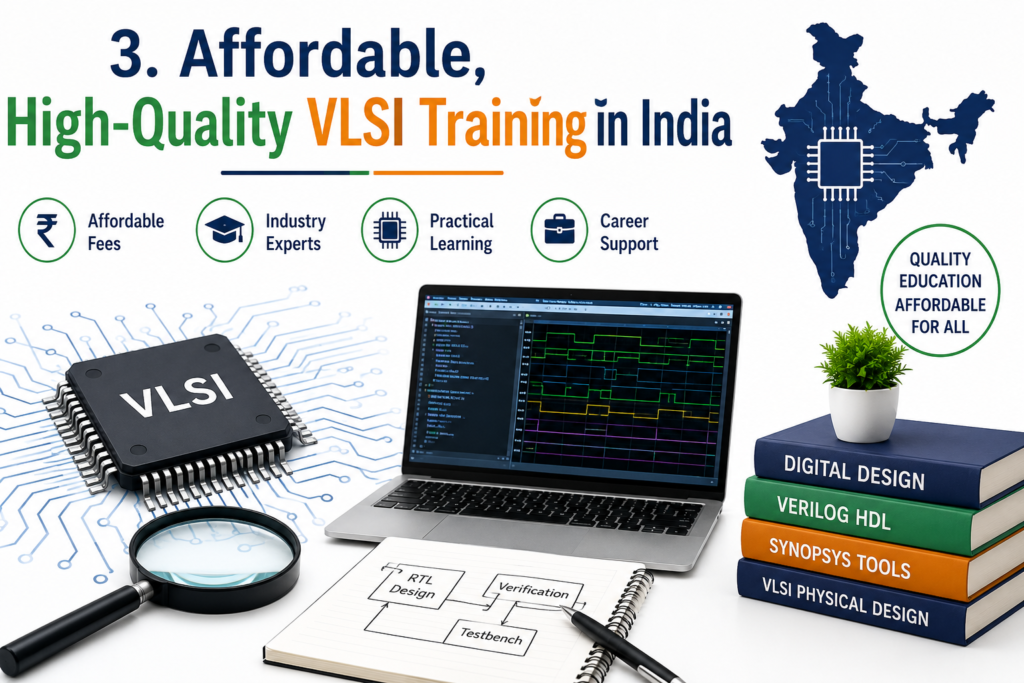
One of the biggest advantages of building a chip design career in India is access to strong, affordable education. Unlike many countries where specialized technical training comes with a hefty price tag, VLSI training in India is available at a fraction of the cost, without compromising on depth or industry relevance.
Programs across the country now cover the full spectrum of the field, including RTL design, functional verification, physical design, design for testability, static timing analysis, and analog layout. Many of these courses are built around the same EDA tools used inside real semiconductor companies, so the transition from classroom to job floor feels far less jarring. Mentorship from professionals who have actual tape-out experience adds another layer of practical value that is hard to find elsewhere at similar cost.
This combination of affordability and quality is exactly why so many people from outside India, and returning professionals from abroad, are choosing to train here before entering the industry.
There is also a growing shift toward flexible learning formats. Weekend batches, evening programs, and blended online-offline courses now make it possible for working professionals to reskill into chip design without stepping away from their current job. This flexibility did not really exist a decade ago, and it has opened the field to a much wider pool of people, not just fresh graduates but also engineers from adjacent fields looking to make a mid-career switch.
4. Strong Salaries, Faster Growth, and Real Job Security

Compensation in this field has improved noticeably over the last few years. Entry-level chip design roles in India commonly start in a solid range, and professionals with a few years of hands-on project experience can see their pay climb significantly, especially in specialized areas like physical design and verification. Beyond the numbers, what stands out is stability: semiconductors are a foundational technology for artificial intelligence, electric vehicles, telecommunications, and consumer electronics, all sectors that are expanding rather than shrinking.
India already contributes a meaningful share of the world’s chip design engineering talent, and that share keeps growing as more design work moves closer to where the manufacturing itself is happening. A widening skills gap in the industry means qualified engineers are not just finding jobs, they are finding multiple offers and genuine room to specialize in the area that interests them most.
Job hopping between design, verification, and physical design roles is also far more common here than in many other engineering fields, largely because the underlying fundamentals overlap. Someone who starts out in verification, for instance, can often move into design or DFT roles a few years in without starting from scratch. That kind of lateral mobility within one industry is rare, and it means fewer people feel stuck in a narrow lane for their entire career.
5. Choosing the Right Institute Matters More Than Ever

With so much opportunity on the table, the real challenge has shifted from “should I enter this field” to “how do I prepare properly for it.” This is where picking the right training path becomes critical. When researching the top 10 VLSI training institutes in India, it helps to look past flashy advertising and focus on a few practical factors: how current the curriculum is, whether the labs give real hands-on exposure to industry-standard EDA tools, how experienced the instructors are, and what the actual placement track record looks like rather than just claimed numbers.
Institutes based in hubs like Bangalore, Hyderabad, and Pune tend to have closer ties to hiring companies simply because of proximity to design centres. Programs that focus deeply on one specialization, such as physical design or verification, often produce more job-ready professionals than generalist courses that try to cover everything lightly. Taking time to compare a handful of programs, read genuine outcomes, and even speak with past trainees before enrolling can make a significant difference in how quickly someone moves from learning to actually working in the industry.
Conclusion
India’s semiconductor story in 2026 is no longer about potential, it is about momentum that is already visible in fabs under construction, in new product launches, and in the sheer number of design centres opening across the country. Between strong government backing, a deep bench of global companies, accessible and high-quality training options, competitive salaries, and genuine long-term demand, few countries offer this complete a package for someone serious about a career in chip design.
Getting in early, choosing the right training path, and specializing in an area that genuinely interests you are the three things that matter most right now. The industry is scaling quickly, and the people who build strong fundamentals today are the ones most likely to be leading design teams a decade from now.
Chip design is not a passing trend riding on hype cycles, it is the quiet infrastructure behind almost every piece of modern technology. Whoever masters it early gets a front-row seat to that infrastructure being built, and right now, India is one of the best places on the map to take that seat.
Why is India the best place to start a VLSI career?
India offers booming semiconductor investments, leading VLSI companies, affordable training, and strong hiring demand, making it ideal for freshers.
Is VLSI a good career in India in 2026?
Yes. India’s semiconductor industry is expanding rapidly, creating thousands of opportunities in RTL Design, Verification, DFT, Physical Design, and Analog.
Which city is best for VLSI jobs in India?
Bengaluru, Hyderabad, Pune, Chennai, and Noida are top VLSI hubs with major semiconductor companies and excellent career opportunities.
Do freshers get VLSI jobs in India?
Yes. Freshers with practical VLSI skills, EDA tool knowledge, and hands-on projects have good chances of getting hired by semiconductor companies.
Which VLSI domain has the highest demand?
RTL Design, Design Verification, Physical Design, DFT, and Analog Layout are among the fastest-growing and most in-demand VLSI domains.