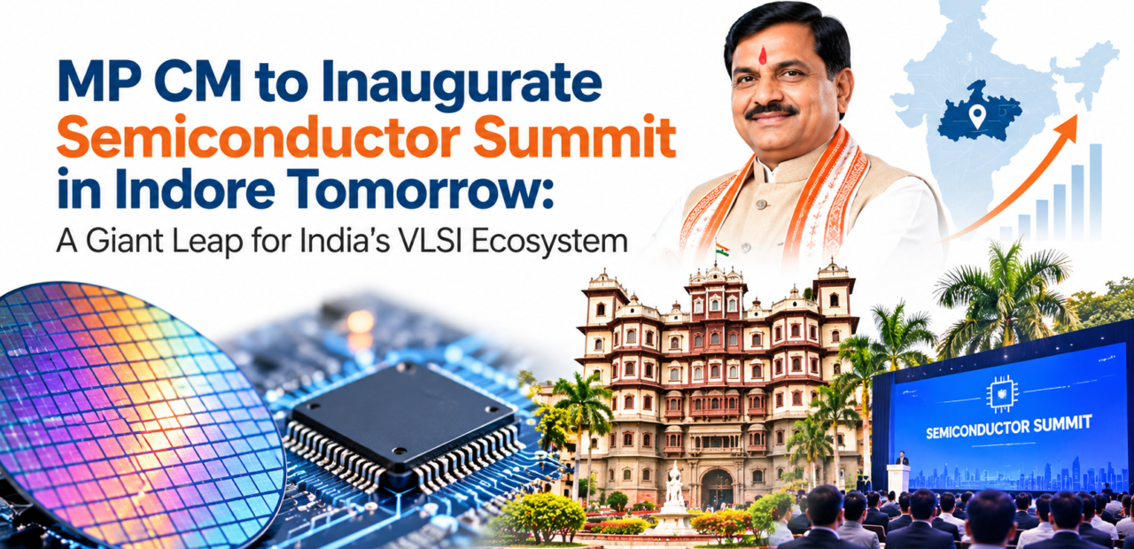
MP CM to Inaugurate Semiconductor Summit in Indore Tomorrow: A Giant Leap for India’s VLSI Ecosystem

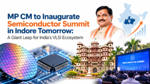
The Indian tech landscape is witnessing a massive transformation as Madhya Pradesh positions itself as a central pillar in the nation’s hardware revolution. Tomorrow, Chief Minister Dr. Mohan Yadav will officially inaugurate the prestigious MP Semiconductor Summit 2026 at the Brilliant Convention Centre in Indore. Bringing together top industry leaders, semiconductor foundries, VLSI design houses, and policymakers, this landmark event marks a decisive step toward turning central India into a premier electronics manufacturing and silicon design ecosystem. The gathering underscores the state’s strategic intent to capture high-value technological investments, build advanced infrastructure, and create a sustainable supply chain for the rapidly evolving microelectronics sector.
As global tech conglomerates search for resilient supply chain destinations, India’s proactive policy support has opened unprecedented pathways for regional industrial expansion. Indore, renowned for its superior connectivity, robust urban infrastructure, and academic excellence, serves as the ideal host for this high-stakes technological assembly. The summit will feature extensive panel discussions, keynotes from global VLSI experts, and interactive roundtables focusing on integrated circuit design, fabless startup acceleration, and advanced testing setups. By organizing this summit, the state leadership demonstrates a clear vision to bridge the gap between academic talent and high-tech manufacturing, ensuring India remains at the forefront of global technological innovation.
Unveiling the State’s Semiconductor Vision and Industrial Policy
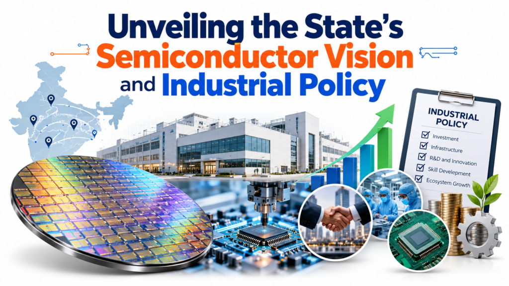
The inauguration by Chief Minister Dr. Mohan Yadav will outline a dedicated roadmap aimed at attracting substantial domestic and foreign direct investments into the high-tech sector. Central to this plan is the MP Semiconductor Policy 2025, which offers capital subsidies up to 25%, subsidized power at promotional rates for a decade, and streamlined single-window clearances for industrial plants. These policy measures significantly reduce entry barriers for semiconductor players.
Through targeted incentives and dedicated industrial parks, the policy supports the establishment of Outsourced Semiconductor Assembly and Test facilities alongside VLSI design centers. By establishing a clear legal and operational foundation, Madhya Pradesh aims to stand out alongside existing technology hubs such as Gujarat, Karnataka, and Tamil Nadu.
Strengthening the Fabless Ecosystem and VLSI Chip Design
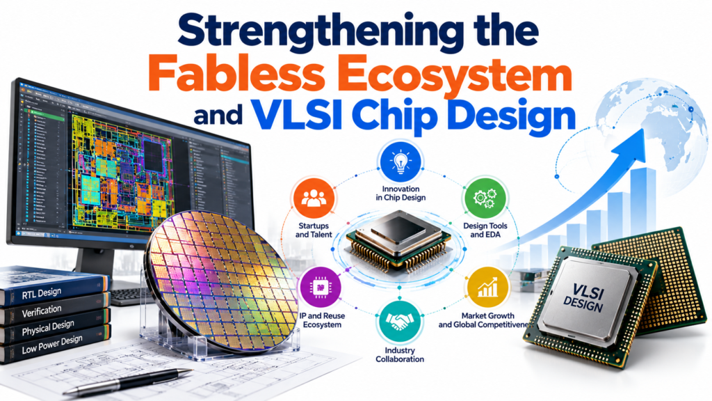
While building silicon fabrication foundries requires heavy capital investment and time, nurturing a robust fabless design ecosystem yields faster regional growth. The summit places a strong emphasis on empowering fabless companies—firms that engineer advanced integrated circuits and system-on-chip architectures while contracting manufacturing out to international foundries.
Promoting chip design allows local technology parks to incubate high-value intellectual property across artificial intelligence, automotive electronics, and telecommunications. Local startups and established engineering firms gain direct exposure to global chip design standards, advanced EDA tools, and venture capital investors, accelerating the commercialization of homegrown silicon solutions.
Attracting OSAT and Advanced Packaging Facilities
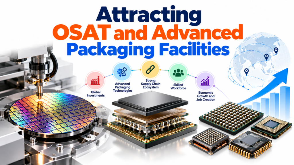
A primary highlight of the summit is attracting investments in Outsourced Semiconductor Assembly and Test facilities and advanced packaging hubs. Among key proposals on the agenda is a massive ₹6,200 crore investment proposal by Paras Semiconductors to establish an OSAT facility within the state.
Assembly, testing, and packaging represent critical stages in turning bare silicon wafers into commercial microchips. Securing functional OSAT facilities establishes immediate industrial capabilities, generates substantial technical employment, and integrates local supply chains directly into global electronics manufacturing ecosystems.
Fostering Industry-Academia Collaboration and Talent Upskilling
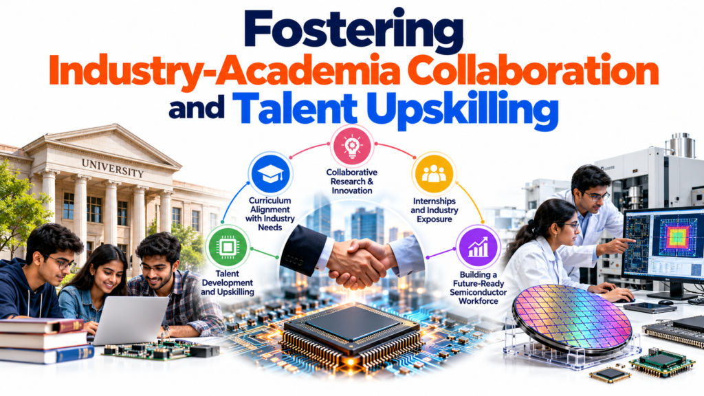
A sustainable semiconductor ecosystem depends on a continuous pipeline of highly skilled VLSI design, testing, and process engineers. The summit facilitates direct engagement between corporate leaders and academic leadership from institutions like IIT Indore, regional engineering colleges, and technical training centers.
Collaborative initiatives aim to modernize engineering curricula, establish state-of-the-art cleanroom laboratories, and introduce targeted certification courses in VLSI layout and verification. This alignment ensures local graduates possess job-ready skills aligned with current industry requirements.
Technological Frontiers: AI Chips, Quantum Computing, and Photonics
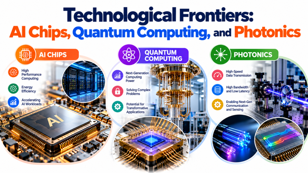
Beyond standard microcontrollers and memory modules, the Indore summit explores advanced hardware frontiers, including AI accelerators, quantum computing hardware, and silicon photonics. Specialized panel sessions will address how specialized domain-specific architectures are reshaping compute efficiency.
By encouraging research and development in photonics and high-performance computing components, Madhya Pradesh prepares its technology landscape for future technological shifts. Nurturing early-stage research in these fields ensures long-term industrial relevance and economic resilience.