

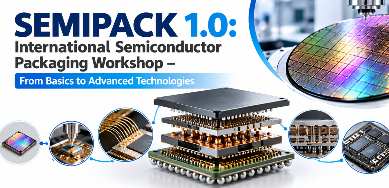
SEMIPACK 1.0: International Semiconductor Packaging Workshop – From Basics to Advanced Technologies

The global semiconductor industry is shifting beyond traditional silicon scaling as advanced packaging becomes essential for improving chip performance, power efficiency, and integration. Modern packaging technologies enable higher-density designs while addressing the rising costs and limitations of conventional semiconductor manufacturing.
SEMIPACK 1.0 is an international semiconductor packaging workshop designed for engineers, researchers, and industry professionals. It covers fundamental assembly techniques, including wire bonding and flip-chip packaging, alongside advanced technologies such as 2.5D and 3D integration and heterogeneous packaging. The workshop provides practical insights into semiconductor packaging innovations and their growing importance in modern VLSI design and manufacturing.
Fundamentals of Traditional Semiconductor Packaging
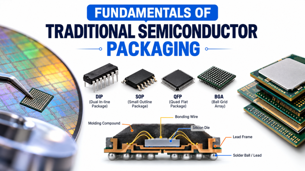
Traditional semiconductor packaging focuses on housing integrated circuits to ensure mechanical protection, electrical connectivity, and environmental isolation. Standard methodologies such as Through-Hole Technology, Surface Mount Technology, and classical Wire Bonding have long provided reliable interconnect solutions for consumer electronics and industrial applications. These foundational approaches rely on leadframes and printed circuit boards to bridge microscopic die pads to system-level circuits, establishing basic operational thermal and electrical pathways.
While cost-effective and highly mature, conventional packaging faces performance bottlenecks as signal speeds increase and form factors shrink. Parasitic inductance, higher electrical resistance, and limited pin counts prevent classical methods from keeping pace with high-frequency VLSI requirements. SEMIPACK 1.0 breaks down these core operational mechanisms to demonstrate where traditional packaging remains viable and precisely where physical constraints demand a transition toward advanced, high-density packaging architectures.
Advanced Packaging Paradigms: 2.5D, 3D, and Heterogeneous Integration
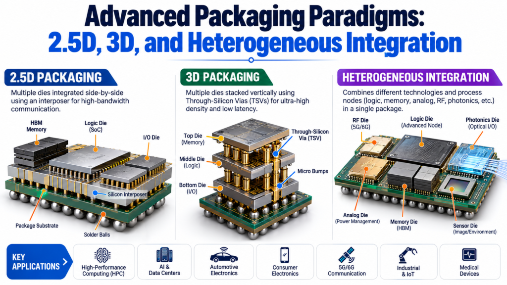
To bypass the limits of monolithic silicon fabrication, the VLSI sector is rapidly adopting heterogeneous integration and multi-die architectures. SEMIPACK 1.0 explores advanced methodologies such as 2.5D interposer structures, 3D IC stacking via Through-Silicon Vias (TSVs), and high-density Fan-Out Wafer-Level Packaging (FOWLP). These technologies enable disparate die modules—such as logic, memory, and analog components—to unite within a single compact package, drastically shortening inter-die interconnect paths.
By replacing long board-level traces with ultra-fine pitch interconnects, advanced packaging minimizes interconnect delay and drastically enhances bandwidth density. Modules at the workshop detail how chiplet architectures leverage hybrid bonding and micro-bumps to achieve functional density comparable to single-die systems. This structural shift redefines system design, allowing engineers to combine nodes optimized for specific tasks while mitigating the yield risks associated with oversized monolithic chips.
Substrate Engineering, Interposers, and High-Density Interconnects
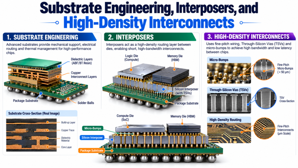
Substrates serve as the physical and electrical foundation of modern semiconductor packages, acting as the critical interface between micro-scale chip pads and macro-scale circuit boards. SEMIPACK 1.0 provides deep technical coverage of substrate materials, ranging from organic laminates and coreless substrates to high-performance silicon and glass interposers. Understanding substrate behavior is crucial for managing signal integrity, controlling line impedance, and mitigating cross-talk in high-speed digital communications.
As interconnect density demands scale upward, fine-pitch routing requires innovative manufacturing processes like semi-additive processing and embedded die technologies. The workshop highlights how silicon interposers enable sub-micron wire traces, while organic and glass alternatives offer cost-effective scaling pathways. Mastery of substrate selection and routing design ensures that integrated packaging systems sustain high data throughput without compromising signal purity or structural robustness.
Thermal Management and Material Reliability Challenges
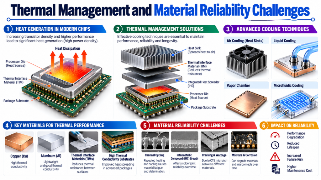
High-density packing of heterogeneous dies significantly raises local thermal flux, placing severe demands on thermal dissipation strategies. SEMIPACK 1.0 addresses the mechanics of heat generation in compact 2.5D and 3D stacks, emphasizing thermal interface materials, heat spreaders, and embedded cooling channels. Without balanced thermal paths, localized hot spots degrade performance, trigger thermal throttling, and cause catastrophic structural failure.
In addition to thermal regulation, mechanical reliability remains a critical engineering priority. Coefficient of Thermal Expansion mismatches between silicon dies, substrates, and molding compounds introduce structural stresses that lead to package warpage, die cracking, and bump fatigue. Workshop sessions examine underfill materials, stress-relief layouts, and finite element reliability modeling, equipping participants with the methodologies needed to build durable integrated packages under harsh operating conditions.
Industrial Implementation, Testing, and Future Packaging Trends
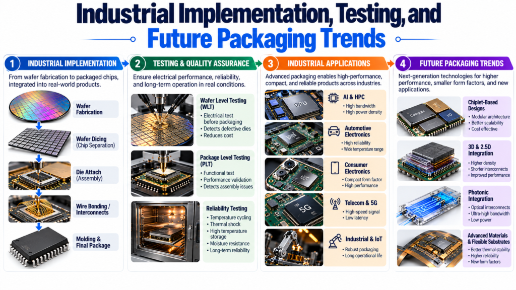
Transitioning advanced packaging designs into high-volume manufacturing requires specialized assembly workflows, strict process controls, and rigorous testing protocols. SEMIPACK 1.0 details industrial process flows, including wafer dicing, high-precision flip-chip placement, reflow soldering, and automated singulation. The workshop underscores Known Good Die testing practices, ensuring that individual chiplets are fully verified prior to integration to avoid compounding yield losses in complex multi-die assemblies.
Looking to the future, semiconductor packaging will drive next-generation innovation across artificial intelligence, high-performance computing, 5G/6G communications, and automotive electronics. Emerging paradigms such as co-packaged optics, panel-level processing, and direct copper-to-copper hybrid bonding are setting new benchmarks for efficiency. SEMIPACK 1.0 delivers a complete, forward-looking roadmap that empowers professionals to adapt to these technological shifts.