
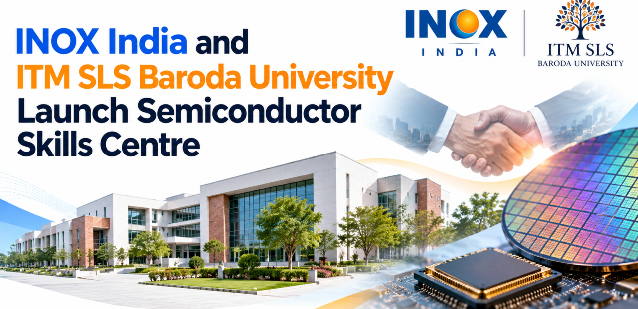
INOX India and ITM SLS Baroda University Launch Semiconductor Skills Centre

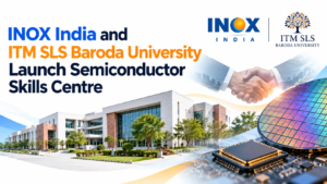
India’s semiconductor industry is expanding beyond chip design and fabrication into the specialised infrastructure required to manufacture advanced electronic components. As investments in semiconductor manufacturing increase, developing a technically skilled workforce has become an important priority. Addressing this need, INOX India Limited (INOXCVA) and ITM SLS Baroda University have inaugurated SemiOrbit, an Orbital Welding and Process Piping Skill Excellence Centre at the university’s Paldi Campus in Vadodara, Gujarat. The centre was inaugurated on 26 October 2026, in collaboration with INOX Air Products and Swagelok Bombay. The initiative focuses on specialised industrial skills that support semiconductor fabrication facilities and advanced electronics manufacturing.
The launch highlights an important aspect of semiconductor development: building the infrastructure and workforce needed to support reliable manufacturing operations. While chip design and fabrication technologies often receive the most attention, semiconductor facilities also depend on specialised gas distribution networks, precision piping and carefully controlled manufacturing environments. SemiOrbit aims to address these requirements through practical training, industry expertise and structured skill development. By connecting academic learning with industrial applications, the initiative seeks to prepare students, trainees and working professionals for technical roles in semiconductor infrastructure and advanced manufacturing.
Understanding the SemiOrbit Semiconductor Skills Centre
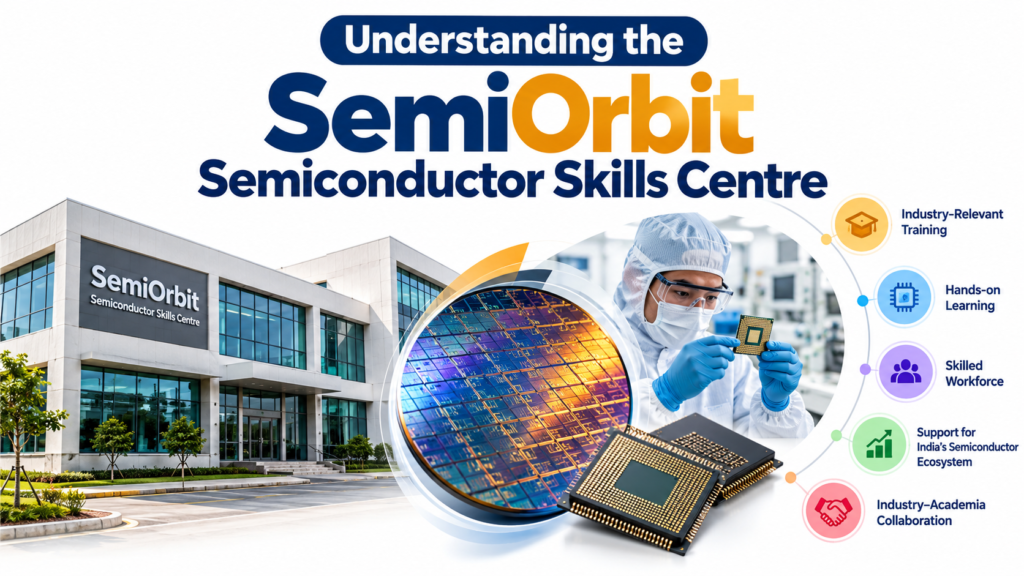
SemiOrbit is a specialised training centre established through collaboration between INOX India and ITM SLS Baroda University, with INOX Air Products and Swagelok Bombay as industry partners. Located at the university’s Paldi Campus in Vadodara, the centre is designed to develop technical capabilities in orbital welding, process piping and semiconductor utility infrastructure. Its primary objective is to help bridge the gap between conventional technical education and the practical requirements of high-precision industrial environments.
The initiative brings together academic training and industry-oriented expertise. Its planned learning approach includes structured training programmes, practical workshops, certification courses and hands-on learning opportunities. These activities are intended to help participants understand the processes, quality expectations and technical standards associated with semiconductor manufacturing infrastructure. The centre is aligned with the broader objectives of the India Semiconductor Mission and India’s efforts to strengthen its domestic semiconductor ecosystem.
Why Orbital Welding and Process Piping Matter
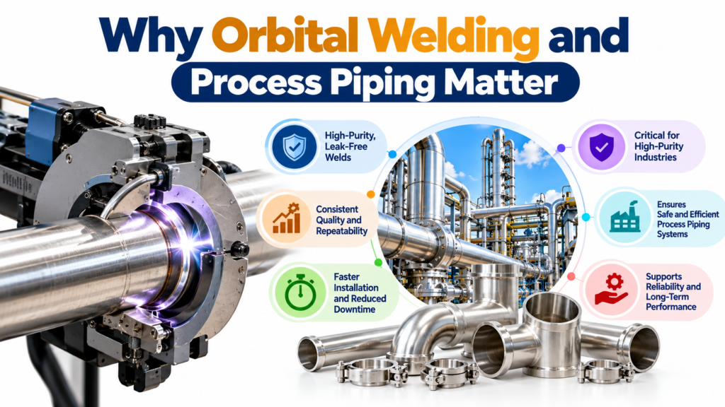
Orbital welding is a mechanised welding process used to create consistent joints around pipes and tubes. In semiconductor facilities, specialised piping systems transport process gases and other utilities that must meet stringent cleanliness and reliability requirements. Weld quality is especially important because imperfections, leaks or contamination can compromise the integrity of systems supporting sensitive manufacturing processes.
Process piping also plays a crucial role in the installation and maintenance of semiconductor utility infrastructure. Engineers and technicians must understand material compatibility, joint quality, inspection procedures and the requirements of ultra-high-purity gas distribution systems. Training in these areas can help build the practical capabilities needed to construct and maintain dependable semiconductor facilities. These skills complement chip design and fabrication expertise rather than replacing them.
Read More: SEMIPACK 1.0: International Semiconductor Packaging Workshop – From Basics to Advanced Technologies
Industry Collaboration and Practical Technical Training
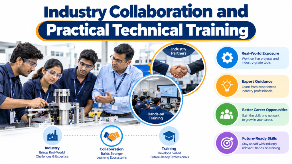
A significant feature of SemiOrbit is the collaboration between educational institutions and industry participants. ITM SLS Baroda University provides the academic setting, while the participating companies contribute expertise related to industrial technologies, gas systems and precision piping. Such collaboration can help training programmes remain connected to the technical requirements encountered in real manufacturing environments.
The centre is intended to support students, trainees and working professionals through practical exposure and specialised learning. Faculty development and industry-oriented training are also part of the broader initiative. However, the centre’s long-term impact will depend on programme implementation, training capacity, assessment methods and the ability to translate acquired skills into relevant employment opportunities. The launch establishes a platform for developing these capabilities, while measurable outcomes will emerge over time.
How the Centre Supports India’s Semiconductor Ambitions
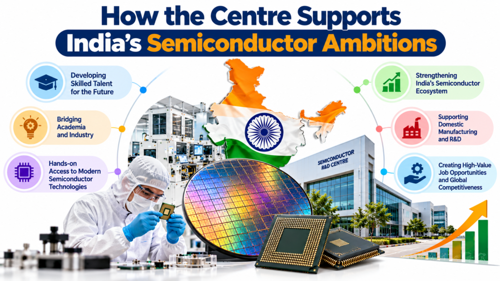
India’s semiconductor ambitions require more than investment in fabrication plants and chip assembly facilities. Manufacturing sites also need dependable utility systems, specialised equipment, trained technicians and professionals who can maintain demanding operational standards. Developing these supporting capabilities is important for establishing an ecosystem that can operate safely, consistently and efficiently.
SemiOrbit contributes to this broader objective by focusing on a specialised segment of semiconductor infrastructure. Its training areas are relevant to the construction, installation and maintenance of systems used in advanced manufacturing. Although the centre alone cannot resolve the industry’s entire skills gap, initiatives that combine technical education with practical industry knowledge can support workforce development. Its contribution will depend on how effectively training aligns with employers’ needs and the industry’s evolving requirements.
Career Opportunities and Future Industry Impact
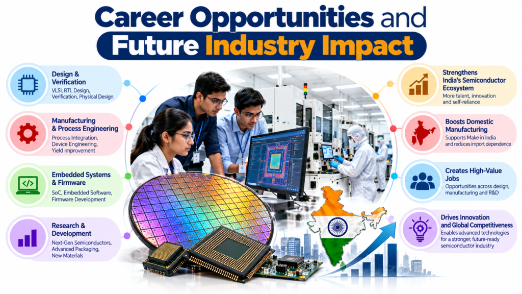
The launch may create additional learning opportunities for people interested in precision welding, industrial piping, gas distribution systems and semiconductor facility infrastructure. Potentially relevant career pathways include orbital welding technician, process piping technician, industrial maintenance technician and specialised fabrication roles. Actual eligibility and job opportunities will depend on employers’ requirements, qualifications, certifications and practical experience.
For students and early-career professionals, the initiative highlights the importance of exploring technical careers beyond semiconductor design and electronics engineering. For existing industrial workers, specialised training may help develop skills relevant to advanced manufacturing environments. As India’s semiconductor ecosystem evolves, industry-aligned education could become an important part of preparing its workforce. Nevertheless, participation in a training programme should not be interpreted as a guarantee of employment or placement.